
Insulated gate bipolar transistor device with low conduction voltage drop, and manufacturing method for insulated gate bipolar transistor device

A technology of bipolar transistors and insulated gates, applied in semiconductor/solid-state device manufacturing, semiconductor devices, electrical components, etc. Problems such as device switching loss, to achieve the effect of strengthening the conductance modulation effect, reducing current, and reducing switching loss

Pending Publication Date: 2017-05-10
WUXI NCE POWER
View PDF6 Cites 12 Cited by
  • Summary
  • Abstract
  • Description
  • Claims
  • Application Information

AI Technical Summary

Problems solved by technology

[0004] However, for the IEGT device structure, 1) due to the use of the dummy trench gate electrode, the device gate capacitance (especially the gate-collector capacitance) is large, but the switching process of the IGBT device is to charge the gate capacitance. , During the discharge process, the larger the gate capacitance is, the longer the discharge time is, and the large gate capacitance (especially the gate-collector capacitance) reduces the switching speed of the device, increases the switching loss of the device, and affects the device. The compromise characteristics of forward voltage drop and switching loss; 2) Due to the existence of the floating body region, the potential in the body is inconsistent during the turn-on and turn-off process of the device, showing large voltage and current oscillations, with Serious EMI problems will seriously affect system reliability

Method used


Image

  • Insulated gate bipolar transistor device with low conduction voltage drop, and manufacturing method for insulated gate bipolar transistor device
  • Insulated gate bipolar transistor device with low conduction voltage drop, and manufacturing method for insulated gate bipolar transistor device
  • Insulated gate bipolar transistor device with low conduction voltage drop, and manufacturing method for insulated gate bipolar transistor device

Examples


Embodiment Construction

[0060] The present invention will be further described below in conjunction with specific drawings and embodiments.

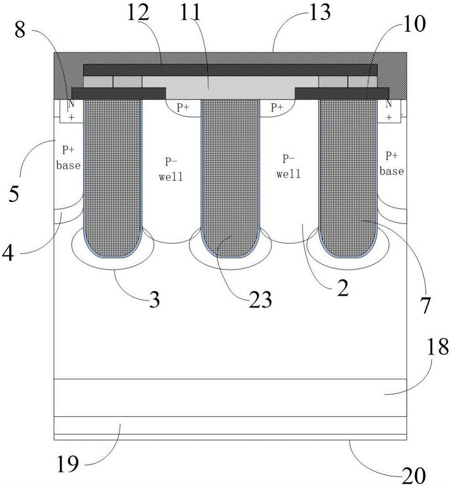
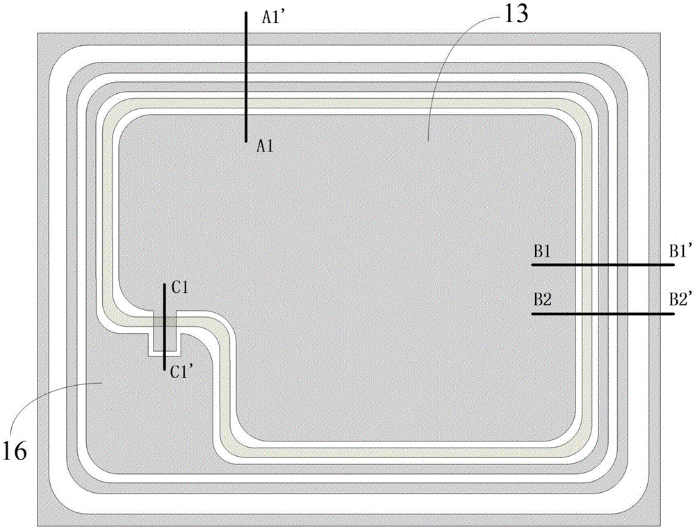
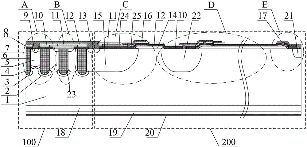
[0061] Such as figure 1 , figure 2 , image 3 , Figure 4 , Figure 5 , Figure 6 and Figure 19 Shown: In order to have extremely low turn-on voltage drop and extremely fast turn-off speed while ensuring withstand voltage, and have low current and voltage oscillations, greatly improving the reliability of work, N-type insulated gate Taking a bipolar transistor device as an example, the present invention specifically includes: on the top view plane of the insulated gate bipolar transistor device, including an active region 100 and a terminal protection region 200 on a semiconductor substrate, the active region 100 Located in the central region of the semiconductor substrate, the terminal protection region 200 is located at the outer ring of the active region 100 and surrounds the active region 100; on the cross-section of the insulated gate bipolar trans...


PUM


Abstract

The invention relates to an insulated gate bipolar transistor device with low conduction voltage drop, and a manufacturing method for the insulated gate bipolar transistor device. The device comprises an active region located on a semiconductor substrate, and a terminal protection region. Active cells of the active region on the section of the device employ a trench structure, and comprise active cells and non-active cells. The bottom of an active cell trench and the bottom of a non-active cell trench are respectively provided with a floating region of a second conductive type, wherein the floating region of the second conductive type below the active cell trench wraps the bottom of the active cell trench, and the floating region of the second conductive type below the non-active cell trench wraps the bottom of the non-active cell trench. The device has extremely low conduction voltage drop and extremely quick cut-off speed under the condition that the withstand voltage is guaranteed, is lower in current and voltage oscillation, and greatly improves the work reliability.

Description

technical field [0001] The invention relates to an insulated gate bipolar transistor device and a manufacturing method thereof, in particular to an insulated gate bipolar transistor device with low conduction voltage drop and a manufacturing method thereof, belonging to the technical field of semiconductor devices. Background technique [0002] The full name of IGBT is Insulate Gate Bipolar Transistor, which is an insulated gate bipolar transistor. It combines multiple advantages of MOSFET and GTR, and greatly expands the application field of power semiconductor devices. As the main representative of new power semiconductor devices, IGBTs are widely used in the fields of industry, information, new energy, medicine, transportation, military and aviation. IGBT is one of the most important power devices at present. Due to the advantages of high input impedance, on-state voltage drop, simple drive circuit, wide safe working area, and strong current handling capacity, IGBT has a...

Claims


Application Information

Patent Timeline
IPC IPC(8): H01L29/739H01L21/331H01L29/06
CPCH01L29/0615H01L29/66325H01L29/7393Y02B70/10
Inventor 朱袁正张硕
Owner WUXI NCE POWER
Learn More