Depositing method for Ag/ZnO/Mg photoelectric transparent conducting thin film

A technology of a transparent conductive film and a deposition method, which is applied in the plating of superimposed layers, ion implantation plating, gaseous chemical plating, etc. The deposition process is easy to control, the preparation process is simple, and the photoelectric properties are excellent.

Inactive Publication Date: 2017-05-10
梁结平
View PDF5 Cites 4 Cited by
  • Summary
  • Abstract
  • Description
  • Claims
  • Application Information

AI Technical Summary

Problems solved by technology

However, it is difficult to prepare high-quality crystalline FTO thin films, and the requirements for the preparation process are high. Due to the existence of internal defects in the thin film, the light transmittance and electrical conductivity are lower than those of ITO thin films; There is some pollution in the process
In addition, due to the high hardness of the FTO film, it is difficult to etch

Method used


Image

  • Depositing method for Ag/ZnO/Mg photoelectric transparent conducting thin film
  • Depositing method for Ag/ZnO/Mg photoelectric transparent conducting thin film
  • Depositing method for Ag/ZnO/Mg photoelectric transparent conducting thin film

Examples


Embodiment 1

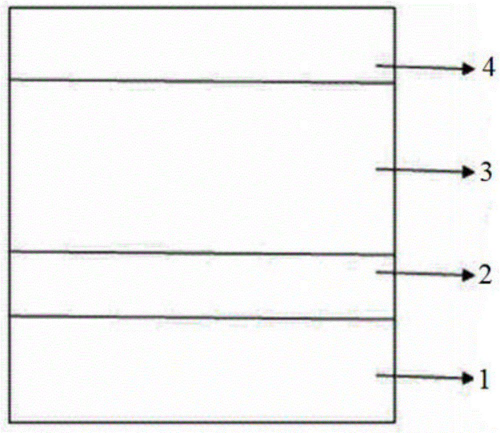
[0023] After the substrate was cleaned with acetone, ethanol and deionized water by ultrasonic waves in sequence, it was blown dry with nitrogen and sent to the reaction chamber.

[0024] Vacuum the background of magnetron sputtering to 9.5×10 -4 After Pa, the substrate was heated to 150° C. and the gas flow rate was adjusted so that the pressure reached 6 Pa, the sputtering power was 150 W, the sputtering time was 2 min, and the thickness of the Mg film was 20 nm.

[0025] Then, the ZnO thin film was deposited and prepared by plasma-enhanced electron cyclotron resonance chemical vapor deposition, and the vacuum was pumped to 7.5×10 -4 After Pa, the substrate was heated to 150°C, and Zn(CH 2 CH 3 ) 2 and O 2 After that, Zn(CH 2 CH 3 ) 2 and O 2 The flow ratio is controlled by a mass flowmeter to be 2sccm: 200sccm, and the total pressure of the gas is controlled to be 1.5Pa; at the electron cyclotron resonance frequency of 750W, the reaction takes 25min to obtain a 450n...

Embodiment 2

[0032] After the substrate was cleaned with acetone, ethanol and deionized water by ultrasonic waves in sequence, it was blown dry with nitrogen and sent to the reaction chamber.

[0033] Vacuum the background of magnetron sputtering to 9.5×10 -4After Pa, the substrate was heated to 150°C and the gas flow rate was adjusted to make the pressure reach 6Pa, the sputtering power was 150W, the sputtering time was 6min, and the thickness of the Mg film was 60nm.

[0034] Then, the ZnO thin film was deposited and prepared by plasma-enhanced electron cyclotron resonance chemical vapor deposition, and the vacuum was pumped to 7.5×10 -4 After Pa, the substrate was heated to 300°C, and Zn(CH 2 CH 3 ) 2 and O 2 After that, Zn(CH 2 CH 3 ) 2 and O 2 The flow ratio is controlled by a mass flowmeter to be 4sccm: 200sccm, and the total pressure of the gas is controlled to be 1.5Pa; at the electron cyclotron resonance frequency of 750W, the reaction takes 45min to obtain a 650nm ZnO thi...


PUM

PropertyMeasurementUnit
thicknessaaaaaaaaaa
thicknessaaaaaaaaaa
electrical resistivityaaaaaaaaaa

Abstract

The invention relates to a depositing method for an Ag/ZnO/Mg photoelectric transparent conducting thin film, and belongs to the field of transparent conducting materials. The depositing method is conducted according to the following steps that (1) a substrate is subjected to ultrasonic cleaning sequentially with acetone, ethyl alcohol and deionized water, then dried with nitrogen and put into a reaction chamber; (2) deposition of a magnetron sputtering Mg film is conducted; (3) a middle layer ZnO thin film is prepared through organic matter chemical vapor deposition; (4) deposition of a magnetron sputtering Ag film is conducted; and (5) the transparent conducting thin film of the Ag/ZnO/Mg multi-layer structure is subjected to high-temperature annealing, the annealing temperature is 200-600 DEG C, the annealing time is 20 min, and the ZnO photoelectric transparent conducting thin film jointly doped with Ag and Mg is obtained. The preparation process is simple, and the depositing process is easy to control. The prepared transparent conducting thin film is good in uniformity and excellent in photoelectric performance, the electrical resistivity can be as low as 7.0*10<-4> ohm.cm, and the light transmittance can reach 85% or above. The transparent conducting thin film can be used for manufacturing transparent electrodes of photoelectric devices such as solar cells, light emitting diodes, LCDs and mobile phones.

Description

technical field [0001] The invention belongs to the field of transparent conductive materials, in particular to a deposition method of Ag / ZnO / Mg photoelectric transparent conductive film. Background technique [0002] With the development of society and the rapid advancement of science and technology, the demand for functional materials is increasing, and new functional materials have become the key to the development of new technologies and emerging industries. With the development of industries such as solar energy, flat panel display and semiconductor lighting, a new functional material - transparent conductive material has been produced and developed. [0003] Transparent conductive film glass is transparent conductive oxide coated glass, which is uniformly coated with a layer of TCO film on the surface of flat glass by physical or chemical coating methods. There are mainly three types of TCO materials in current application, ITO-In2O3 based thin film (Sn doped), FTO-Sn...

Claims


Application Information

Patent Timeline
Patent Type & Authority Applications(China)
IPC IPC(8): C23C28/00C23C14/35C23C14/18C23C14/20C23C16/40C23C14/58
CPCC23C28/322C23C14/185C23C14/205C23C14/35C23C14/5806C23C16/407C23C28/345
Inventor 梁结平
Owner 梁结平
Why Eureka
Try Eureka