Processing method of conductive plasticine used for fixing SEM (Scanning Electron Microscope) sample

A technology of electron microscopy and conductive rubber, which is applied in the direction of conductive materials dispersed in non-conductive inorganic materials, cable/conductor manufacturing, circuits, etc., and can solve the problems of polluting microscope lenses and conductive powder falling off

Active Publication Date: 2017-03-29
ZHEJIANG IND & TRADE VACATIONAL COLLEGE
View PDF3 Cites 2 Cited by
  • Summary
  • Abstract
  • Description
  • Claims
  • Application Information

AI Technical Summary

Problems solved by technology

Metallographic plasticine can fix special-shaped parts very well, which is convenient for metallographic observation, but it is not conductive; invention patent: a method of enhancing the conductivity of plasticine for children's toys (publication number 105268198A) is to add plasticine to plasticine Conductive powder, and SEM analysis needs to be carried out under high vacuum. The conductive powder in the plasticine may fall off and contaminate the microscope lens; Invention patent: vertical hanging demonstration teaching aid for circuit teaching based on plasticine as a wire (public number 105931542A) The conductive plasticine used is to add salt water to the plasticine. The same SEM analysis requires a dry and clean environment to avoid volatilization, so the above two conductive plasticines are not suitable.

Method used


Image

  • Processing method of conductive plasticine used for fixing SEM (Scanning Electron Microscope) sample
  • Processing method of conductive plasticine used for fixing SEM (Scanning Electron Microscope) sample
  • Processing method of conductive plasticine used for fixing SEM (Scanning Electron Microscope) sample

Examples


Embodiment Construction

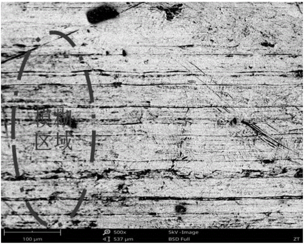
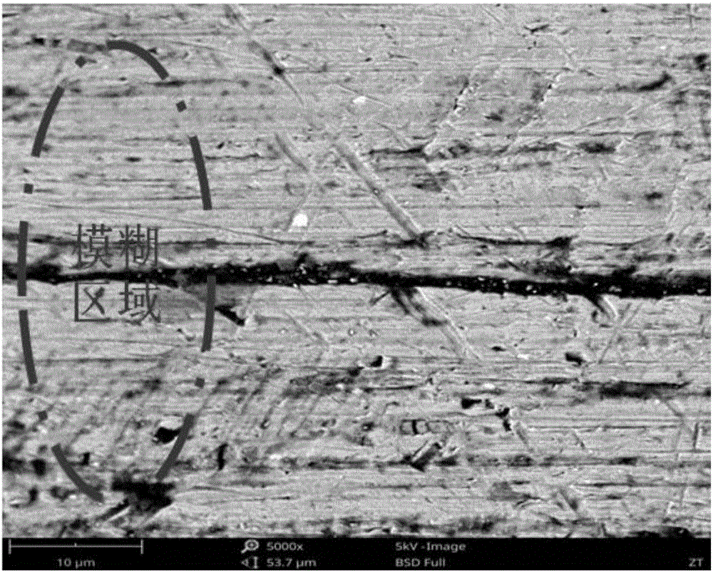
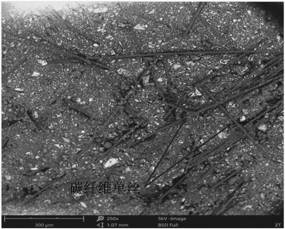
[0013] Specific embodiments of the present invention such as Figure 1-4 Shown is the processing method of conductive plasticine for fixing scanning electron microscope samples, which is characterized in that it includes the following steps: ① using metallographic plasticine, heating it to 25 ° C, ② placing the plasticine on a smooth glass plane , use a round stick to flatten it to a sheet with a thickness of 1mm, ③sprinkle 1cm long carbon fiber monofilament without sizing and glue on the surface of the sheet, the carbon content of carbon fiber is ≥95%, and the resistivity is ≤1.5×10 ﹣3 Ωcm, carbon fiber monofilaments overlap each other to form a staggered two-dimensional structure, and then use a round stick to gently press the carbon fiber into the plasticine. ④ Gently brush the surface of the plasticine with a soft brush to remove unfixed carbon fiber monofilaments , ⑤For the position where carbon fiber monofilaments are sparsely distributed on the surface, repeat ③~④ to en...


PUM

PropertyMeasurementUnit
Lengthaaaaaaaaaa

Abstract

The invention discloses a processing method of conductive plasticine used for fixing an SEM sample. The method comprises the following steps that metallographic plasticine is heated, placed on a smooth glass plane and evened out into a slice, non-pasted non-gel long single carbon fibers are sprinkled on the slice, the single carbon fibers are overlapped with one another to form an interlaced 2D structure, a roller presses the carbon fibers into the plasticine lightly, it is ensured that the surface of the plasticine is adhered with the overlapped single carbon fibers uniformly, and the plasticine whose surface is adhered with the overlapped single carbon fibers uniformly is rolled into a cylindrical shape and then evened out into a slice along the vertical direction. The carbon fibers are added in a layered manner for multiple times and then extruded in an anisotropic manner, a 3D conductive structure communicated with each other is formed among the long single carbon fibers added to the metallographic plasticine, cumulative charges are eliminated effectively, and the conductive plasticine can fix an irregular piece or an inclined side of the sample effectively, and is suitable for use of the SEM.

Description

technical field [0001] The invention belongs to the technical field of experimental equipment, in particular to a processing method of conductive plasticine used for fixing scanning electron microscope samples. Background technique [0002] Scanning Electron Microscope (SEM) is a means of observing microscopic properties between the transmission electron microscope and the optical microscope. It can directly use the material properties of the sample surface material for microscopic imaging. The advantages of the scanning electron microscope are: (1) high magnification; (2) large depth of field, large field of view, and three-dimensional imaging, which can directly observe the fine structure of the uneven surface of various samples. Scanning electron microscopy (SEM) mainly uses secondary electron signal imaging to observe the surface morphology of samples. When the sample resistance is large, under the continuous scanning of the electron beam, the surface of the sample grad...

Claims


Application Information

Patent Timeline
IPC IPC(8): H01B13/00H01B1/24
CPCH01B1/24H01B13/00
Inventor 王坤童先魏爱平林继兴史子木刘东华
Owner ZHEJIANG IND & TRADE VACATIONAL COLLEGE
Why Eureka
Try Eureka