Superhard diamond-like carbon antireflection coating, infrared material with antireflection coating, preparation method and application thereof
A technology of diamond-like film and infrared material, applied in the field of infrared material and its preparation, superhard diamond-like carbon anti-reflection film, can solve the problems of infrared window resistance to heavy friction and high-speed sand wear limitation, and achieve strong resistance to chemical factors such as seawater and other long-term The effect of corrosion, strong high-speed sand erosion, and resistance to heavy friction and high-speed sand erosion
- Summary
- Abstract
- Description
- Claims
- Application Information
AI Technical Summary
Problems solved by technology
Method used
Image
Examples
Embodiment 1
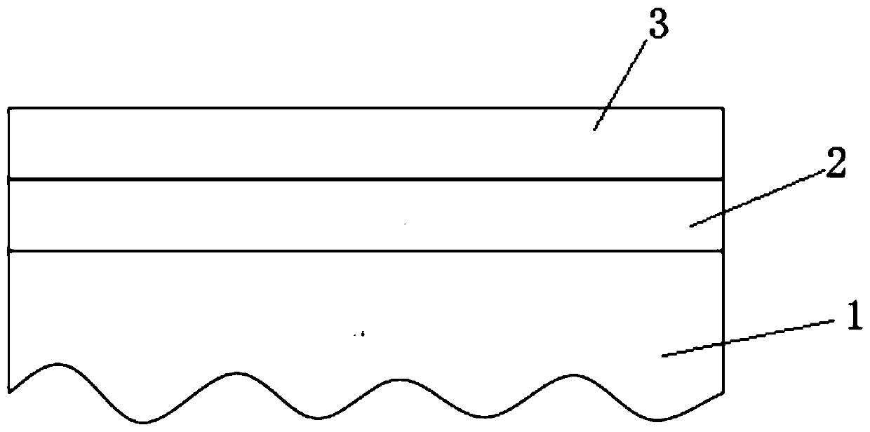
[0035] Plating a-C:H / ta-C double-layer superhard diamond-like film on the Ge substrate is anti-reflection in the 8-12μm segment, and the center wavelength is 9μm. If the thickness of the two films is the same, the refractive index of a-C:H 2. The refractive index of ta-C is 2.7, and the physical thickness of the two films is 475nm, such as figure 1 shown.
[0036] (1) Use a dust-free cloth to polish the double-sided Φ50×2 Ge substrate, drop alcohol and wipe it under strong light.
[0037] (2) Put the substrate on the lower plate of the PECVD equipment and vacuumize to 3×10 -3 Pa, adjust the radio frequency power 200-2000w, plate the bottom a-C:H film, and the plating time is 10min.
[0038] (3) Place the substrate coated with a-C:H film on the target holder of the FCVA equipment so that it forms an angle of 45° with the beam. Adjust the bias voltage and the size of the arc current, and plate a ta-C film on the a-C:H film for 55 minutes.
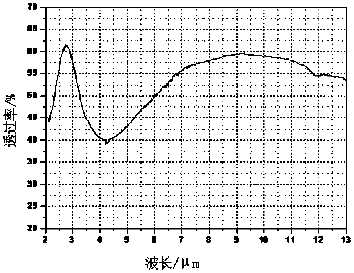
[0039] (4) The transmittance test ...
Embodiment 2
[0045] The a-C:H / ta-C double-layer superhard diamond-like film is plated on the Ge substrate to increase the reflection in the 8-12μm segment, and the center wavelength is 9μm. According to the film system design software Essential Macleod software design, the refractive index of a-C:H 2, the physical thickness is 794nm, the refractive index of ta-C is 2.7, and the physical thickness is 213nm.
[0046] (1) Use a dust-free cloth to polish the double-sided Φ60×2 Ge substrate, drop alcohol and wipe it under strong light.
[0047](2) Put the substrate on the lower plate of the PECVD equipment and vacuumize to 3×10 -3 Pa, adjust the radio frequency power to 200-2000w, plate the bottom a-C:H film, and the plating time is 18min.
[0048] (3) Place the substrate coated with a-C:H film on the target holder of the FCVA equipment so that it forms an angle of 45° with the beam. Adjust the bias voltage and the size of the arc current, and plate a ta-C film on the a-C:H film for 25 minute...
Embodiment 3
[0051] Plating a-C:H / ta-C double-layer superhard diamond-like film on the Si substrate is anti-reflection in the 3-5μm segment, and the center wavelength is 4μm. If the thickness of the two films is the same, the refractive index of a-C:H is 2, The physical thickness is 212nm, the refractive index of ta-C is 2.7, and the physical thickness is 212nm.
[0052] (1) Wipe the double-sided polished Φ55×2 Si substrate with a dust-free cloth dipped in alcohol under strong light.
[0053] (2) Put the substrate on the lower plate of the PECVD equipment and vacuumize to 3×10 -3 Pa, adjust the radio frequency power to 200-2000w, plate the bottom a-C:H film, and the plating time is 8.6min.
[0054] (3) Place the substrate coated with a-C:H film on the target holder of the FCVA equipment so that it forms an angle of 55° with the beam. Adjust the bias voltage and the size of the arc current, and plate a ta-C film on the a-C:H film for 9.4 minutes.
[0055] (4) a-C:H / ta-C double-layer film...
PUM
| Property | Measurement | Unit |
|---|---|---|
| thickness | aaaaa | aaaaa |
| hardness | aaaaa | aaaaa |
| hardness | aaaaa | aaaaa |
Abstract
Description
Claims
Application Information
 - Generate Ideas
- Intellectual Property
- Life Sciences
- Materials
- Tech Scout
- Unparalleled Data Quality
- Higher Quality Content
- 60% Fewer Hallucinations
Browse by: Latest US Patents, China's latest patents, Technical Efficacy Thesaurus, Application Domain, Technology Topic, Popular Technical Reports.
© 2025 PatSnap. All rights reserved.Legal|Privacy policy|Modern Slavery Act Transparency Statement|Sitemap|About US| Contact US: help@patsnap.com


