
Hybrid surface-mounting process of double-side board

A double-sided, mounting technology, applied in the direction of assembling printed circuits with electrical components, metallurgical bonding, electrical components, etc., can solve the problems of increasing production costs, slow curing speed, low product qualification rate, etc., to achieve production efficiency and product qualification. The effect of improving the rate of production, reducing the production cost and high product qualification rate

Inactive Publication Date: 2017-02-15
WUXI NASCH CONTROL & TEST TECH
View PDF0 Cites 15 Cited by
  • Summary
  • Abstract
  • Description
  • Claims
  • Application Information

AI Technical Summary

Problems solved by technology

[0004] In the process of PCB board production, mixed assembly refers to the assembly method of both placement and insertion. It combines the advantages of placement and insertion and is more and more perfused by enterprises. The double-sided mixed assembly in the prior art Chip technology has defects such as complicated process, low product qualification rate, low efficiency, low bonding strength of patch adhesive, and slow curing speed, especially for some products with large PCB boards, many components, and high integration, such as If the quality of the patch cannot be guaranteed, it will affect the production efficiency and product qualification rate, and directly increase the production cost

Method used


Image

  • Hybrid surface-mounting process of double-side board

Examples


Embodiment Construction

[0038] The technical solutions of the present invention will be further described in detail below in conjunction with specific embodiments.

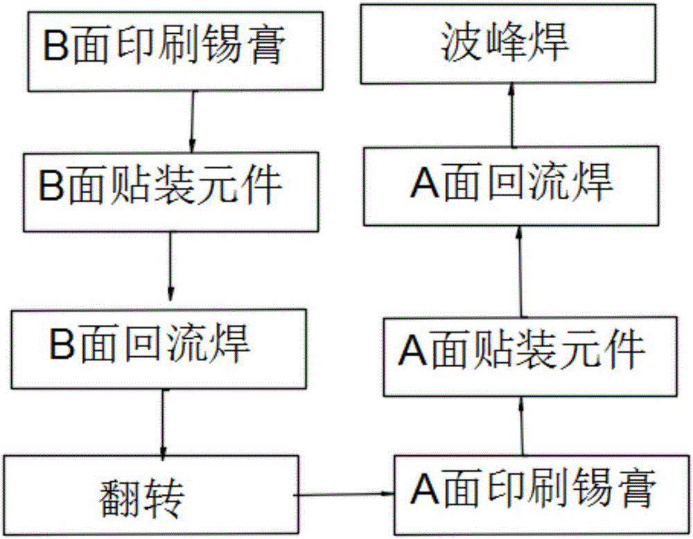
[0039] A double-sided mixed mounting process, the steps are as follows:

[0040] S1: Printing solder paste on the B side; using the stencil as the printing plate, the solder paste is printed onto the pads on the B side of the PCB board under the push of a scraper. The equipment used is a solder paste printing machine, which is located at the end of the SMT production line. front end;

[0041] S2: B surface mount components; it is to accurately install the surface mount components to the fixed position of the B surface of the PCB board. The equipment used is a placement machine, which is installed behind the printing machine in the SMT production line.

[0042] S3: B-side reflow soldering; apply a controlled amount of solder paste and solvent on the surface to be connected, then place the components in their positions, and then increase...


PUM


Abstract

The invention discloses a hybrid surface-mounting process of a double-side board. The hybrid surface-mounting process comprises the steps of S1, printing tin paste on a B surface, in which the tin paste is printed on a bonding pad on the B surface of a PCB (Printed Circuit Board) under push of a scraper; S2, surface-mounting a component on the B surface, in which a surface-mounted component is accurately arranged on a fixed position of the B surface of the PCB; S3, performing reflow soldering on the B surface, in which quantity-controllable tin paste and a solvent are applied onto a surface to be connected, the component is placed on positions of the tin paste and the solvent, and the tin paste is molten by increasing a temperature and heating so that the surface-mounted component and the B surface of the PCB are firmly bonded; S4, performing turnover, in which the circuit board is turned over to complete printing of an A surface; S5, printing the tin paste on the A surface; S6, surface-mounting a component on the A surface; S7, performing reflow soldering on the A surface; and S8, performing wave soldering, in which molten soft welding material is sprayed by a power-driven pump or an electromagnetic pump to form a soldering material wave required by design so that a welding end or a pin of the component and the bonding pad of the printed circuit board are welded. The hybrid surface-mounting process of the double-side board is simple, the qualified rate of a product is high, and the curing speed is fast.

Description

technical field [0001] The invention relates to the technical field of circuit boards, in particular to a double-panel mixed mounting and mounting process. Background technique [0002] PCB board is also called circuit board, printed circuit board and so on. The PCB board makes the circuit miniaturized and intuitive, and plays an important role in mass production of fixed circuits and optimizing the layout of electrical appliances. According to the number of layers, circuit boards are divided into three major categories: single-panel, double-panel, and multi-layer circuit boards. On the most basic PCB, parts are concentrated on one side, and wires are concentrated on the other side. Because wires only appear on one side, this PCB is called a single-sided circuit board. Double-sided panels are an extension of single-sided panels. When single-layer wiring cannot meet the needs of electronic products, double-sided panels must be used. Both sides of the double-sided board ha...

Claims


Application Information

Patent Timeline
IPC IPC(8): H05K3/34
CPCH05K3/341H05K3/3447H05K2201/10545H05K2203/04
Inventor 杨海江马星河
Owner WUXI NASCH CONTROL & TEST TECH
Learn More