
Rectifying device and preparation method thereof

A technology of rectifier devices and devices, which is applied in semiconductor/solid-state device manufacturing, electric solid-state devices, semiconductor devices, etc., can solve the problems of low forward conduction voltage drop, high blocking voltage, current leakage, and high turn-on voltage of PN junction diodes. Achieve the effect of reducing production cost and simple steps

Inactive Publication Date: 2017-02-15
WUXI CHINA RESOURCES HUAJING MICROELECTRONICS
View PDF6 Cites 3 Cited by
  • Summary
  • Abstract
  • Description
  • Claims
  • Application Information

AI Technical Summary

Problems solved by technology

[0006] The purpose of the present invention is to propose a rectifying device and a preparation method thereof. The rectifying device has a lower forward conduction voltage drop and a high blocking voltage, which can solve the problem of high turn-on voltage of the existing PN junction diode as a rectifying device. Schottky diodes have low reverse withstand voltage and have problems with current leakage

Method used


Image

  • Rectifying device and preparation method thereof
  • Rectifying device and preparation method thereof
  • Rectifying device and preparation method thereof

Examples


Embodiment 1

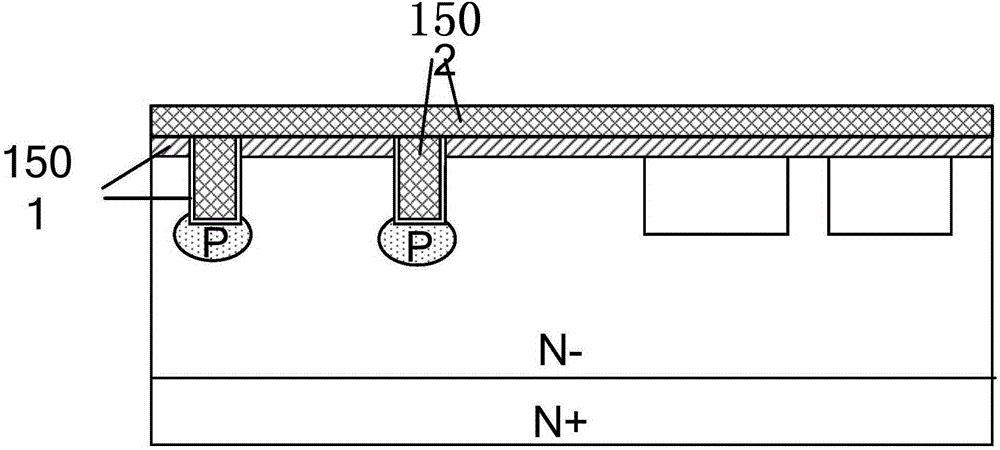
[0054] A rectifier device provided by Embodiment 1 of the present invention, the device includes a substrate of the first conductivity type, a cell region and a terminal region; a groove-shaped region is provided on the front of the substrate of the cell region; There is a second conductivity type buried layer region; the remaining area of ​​the substrate front of the cell region except the trench type region is provided with a second conductivity type body region; the substrate front of the cell region is provided with a first metal electrode; the substrate The back is provided with a second metal electrode.

[0055] Wherein, the terminal region includes a terminal structure, and the terminal structure can specifically be a field-limiting ring, a field-limiting ring plus a field plate, a terminal structure prepared by a junction termination extension (JTE) technology, or a laterally variable doping (VLD) In this embodiment, the terminal structure and the like prepared by the ...

Embodiment 2

[0065] An embodiment of the present invention provides a method for manufacturing a rectifier device. The method includes: forming a termination region on the front surface of a substrate of the first conductivity type, and the remaining region on the front surface of the substrate except the termination region is a cell region; A trench-type region, a buried layer region of the second conductivity type, and a body region of the second conductivity type, wherein the trench-type region is arranged on the substrate front side of the cell region, and the buried layer region of the second conductivity type is arranged on the surface of the trench-type region At the bottom, the body region of the second conductivity type is arranged on the remaining area of ​​the substrate front of the cell region except for the trench type region; the first metal electrode is prepared on the substrate front of the cell region; the second metal electrode is prepared on the back of the substrate meta...


PUM

PropertyMeasurementUnit
Thicknessaaaaaaaaaa

Abstract

The present invention discloses a rectifying device and a preparation method thereof. The device comprises a substrate of a first conductive type, a cell area and a terminal area, wherein a groove type area is arranged on the right side of the substrate of the cell area, the bottom of the groove type area is equipped with a buried layer area of a second conductive type, and the rest areas of the right side of the substrate of the cell area except the groove type area are equipped with the body areas of the second conductive types. The rectifying device contains an MOS structure and a PN junction simultaneously, the advantages of the MOS device and a PN diode can be combined together, and by a groove type structure, the junction type field effect transistor parasitic resistance is not generated, the reduction of the positive conduction voltage drop is not limited, at the same time, the channel density of the device in the unit area also can be increased, and the device cost is reduced. The buried layer area of the second conductive type at the bottom of the groove type area enables a blocking voltage to be improved effectively. Therefore, the rectifying device is simple in structure and excellent in performance, and also has the low positive conduction voltage drop and the high blocking voltage.

Description

technical field [0001] The invention relates to the technical field of semiconductors, in particular to a rectifier device and a preparation method thereof. Background technique [0002] Semiconductor diodes have the characteristics of forward conducting and reverse blocking, and are widely used in various electronic circuits such as power supplies and signal processing. For a specific type of diode device, the forward current is basically negligible until the forward bias voltage reaches a certain value (forward conduction voltage drop, also known as forward voltage drop). Traditional rectifier diodes mainly include PN junction diodes and Schottky diodes. The PN junction diode has a large forward voltage drop VF and a long reverse recovery time Trr, but the PN junction diode has good stability and can work at high voltage; Schottky diodes are made of precious metals (such as gold, silver, titanium, etc.) etc.) are in contact with semiconductors to form heterojunction barr...

Claims


Application Information

Patent Timeline
IPC IPC(8): H01L27/06H01L29/78H01L29/861H01L29/06H01L21/77
Inventor 钟圣荣邓小社周东飞
Owner WUXI CHINA RESOURCES HUAJING MICROELECTRONICS
Learn More