High dynamic focal plane readout circuit and sampling method thereof
A readout circuit and focal plane technology, applied in the field of detection, can solve the problems that it is difficult to achieve high dynamic range, the number of equivalent noise electrons is large, and cannot be satisfied at the same time, and achieve small readout noise, small noise electron number, The effect of high conversion gain
- Summary
- Abstract
- Description
- Claims
- Application Information
AI Technical Summary
Problems solved by technology
Method used
Image
Examples
Embodiment 1
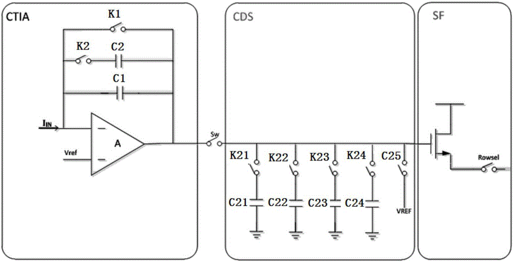
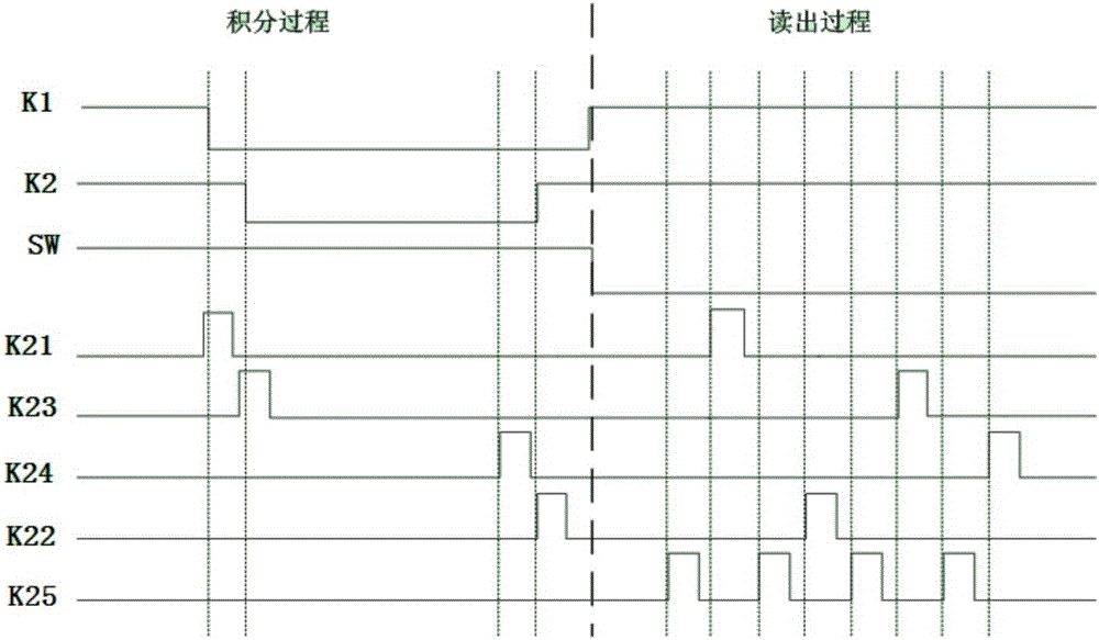
[0042] Such as figure 2As shown, the high dynamic range focal plane readout circuit of the present invention includes a capacitive transconductance amplifier CTIA, a sampling circuit CDS, a source follower SF; the capacitive transconductance amplifier CTIA includes an amplifier A and a signal voltage connected in parallel across the amplifier A The amplifier reset switch K1 and the first integration capacitor C1 between the input terminal and the output terminal, the low gain enable switch K2 and the second integration capacitor C2; the low gain enable switch K2 and the second integration capacitor C2 are connected in series across the amplifier A Between the signal voltage input terminal and the output terminal; the sampling circuit CDS is connected to the output terminal of the amplifier A through the isolation switch SW; the switch Sw is used to isolate the capacitive transconductance amplifier CTIA and the sampling circuit CDS, and can realize integration while reading Fu...
Embodiment 2
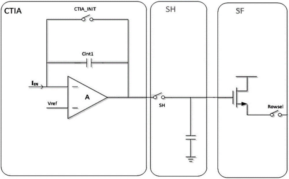
[0055] Such as Figure 4 As shown, the high dynamic range focal plane readout circuit of the present invention includes a capacitive transconductance amplifier CTIA, a sampling circuit SH, a source follower SF; the capacitive transconductance amplifier CTIA includes an amplifier A and a signal voltage connected in parallel across the amplifier A The amplifier reset switch K1 and the first integration capacitor C1 between the input terminal and the output terminal, the low gain enable switch K2 and the second integration capacitor C2; the low gain enable switch K2 and the second integration capacitor C2 are connected in series across the amplifier A between the input terminal and the output terminal; the sampling circuit SH is connected to the output terminal of the amplifier A through the isolating switch SW; the isolating switch Sw is used to isolate the capacitive transconductance amplifier CTIA and the sampling circuit SH, and can realize the integration function while readi...
PUM
 Abstract
Description
Claims
Application Information
 - R&D
- Intellectual Property
- Life Sciences
- Materials
- Tech Scout
- Unparalleled Data Quality
- Higher Quality Content
- 60% Fewer Hallucinations
Browse by: Latest US Patents, China's latest patents, Technical Efficacy Thesaurus, Application Domain, Technology Topic, Popular Technical Reports.
© 2025 PatSnap. All rights reserved.Legal|Privacy policy|Modern Slavery Act Transparency Statement|Sitemap|About US| Contact US: help@patsnap.com


