Conical interdigital DNA double helix bionic left-handed material
A left-handed material, double helix technology, used in electrical components, antennas, etc., can solve the problems of low practical value, complexity, and many adjustment restrictions, and achieve the effect of convenient production and later loading and application.
- Summary
- Abstract
- Description
- Claims
- Application Information
AI Technical Summary
Problems solved by technology
Method used
Image
Examples
Embodiment 1
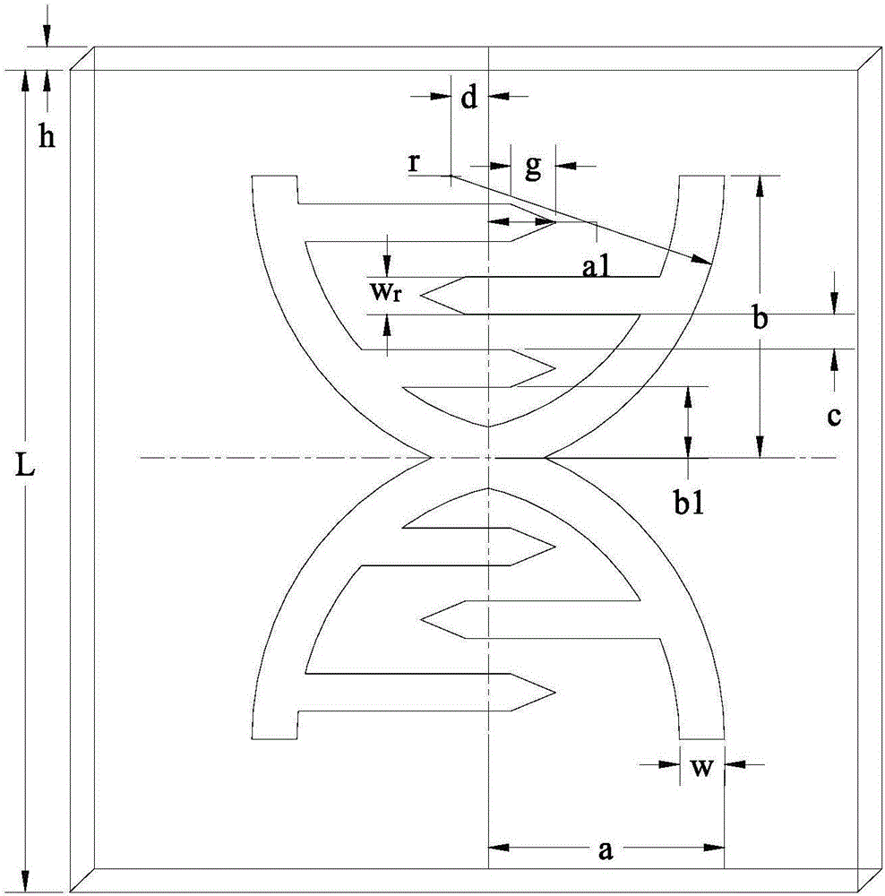
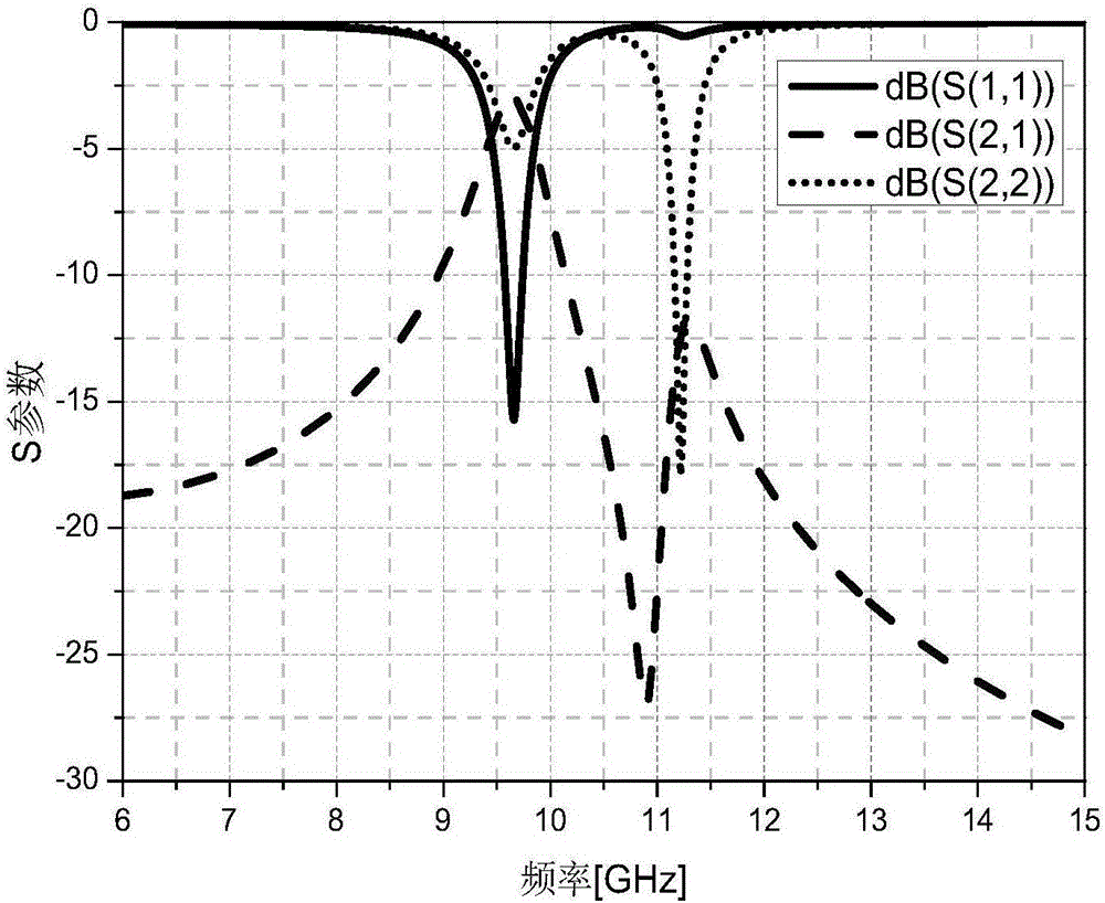
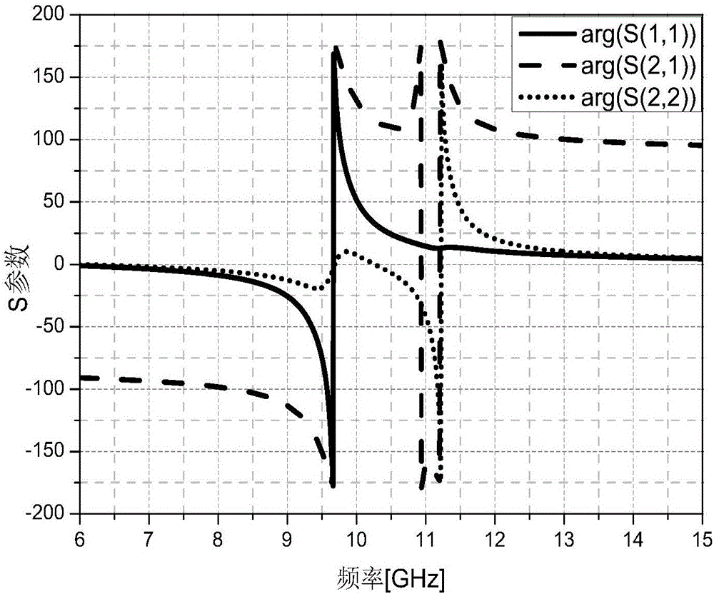
[0039] Embodiment 1: see figure 1 , the basic structure of the present invention is a high-performance dielectric substrate covered with a good conductor on one side. Conductor thickness is 0.017mm. On the surface of the good conductor of the dielectric substrate, two pairs of upper and lower crossed symmetrical spiral metal wires are etched, showing a mirror image symmetrical structure, and the upper and lower sides are connected by interdigitated metal rods. The cross-symmetrical spiral metal wires are all composed of circular arcs. The center of the circular arc deviates slightly from the left and right central axes, the distance d from the central axis is 0.5mm, and the distance b from the horizontal axis is 2.4mm. The radius r of the outer arc of the spiral metal wire is 2.6 mm; the inner arc is a concentric structure, and the distance w between the inner and outer arcs is 0.4 mm. On the inside of each pair of intersecting double helixes, an inward interdigitated arm ex...
Embodiment 2
[0042] Example 2: see Figure 9 , on the basis of the original unit structure, this embodiment changes the tapered tail of the interdigitated structure into a circular hole with a radius of r1=0.12mm on the finger arm of the interdigitated capacitor, so as to increase the number of fingers in the interdigitated structure. series inductance. And opening holes in the fingers of the interdigitated capacitor can obviously change the current path in the interdigitated structure, thus changing the electromagnetic properties of the left-handed material. Such as Figure 10 As shown, the dual negative frequency bands of this embodiment are from 10.30 GHz to 12.30 GHz, and the bandwidth is obviously increased.
PUM
| Property | Measurement | Unit |
|---|---|---|
| Side length | aaaaa | aaaaa |
| Thickness | aaaaa | aaaaa |
| Thickness | aaaaa | aaaaa |
Abstract
Description
Claims
Application Information
 - R&D
- Intellectual Property
- Life Sciences
- Materials
- Tech Scout
- Unparalleled Data Quality
- Higher Quality Content
- 60% Fewer Hallucinations
Browse by: Latest US Patents, China's latest patents, Technical Efficacy Thesaurus, Application Domain, Technology Topic, Popular Technical Reports.
© 2025 PatSnap. All rights reserved.Legal|Privacy policy|Modern Slavery Act Transparency Statement|Sitemap|About US| Contact US: help@patsnap.com


