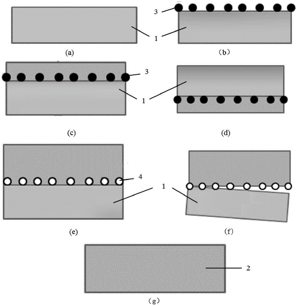
Preparation method of GaN substrate
A technology of substrates and composite substrates, which is applied in the manufacture of semiconductor/solid-state devices, semiconductor devices, electrical components, etc., can solve the problems of low crystal quality and yield of GaN substrate materials, complicated processes, etc., and achieve the convenience of large-scale batch production The production and preparation methods are simple and the price is low
- Summary
- Abstract
- Description
- Claims
- Application Information
AI Technical Summary
Problems solved by technology
Method used
Image
Examples
Embodiment 1
[0029] Embodiment 1. Preparation of c-plane self-supporting GaN substrate:
[0030] 1) The substrate can be a sapphire substrate, or a thin film of GaN, AlN, InN or other III-nitride materials grown on a sapphire substrate; the carbon nanotubes are arranged in parallel along the growth plane, and the arrangement is It can be an isoperiodic or periodic disordered structure. Carbon nanotubes can be a single carbon nanotube or a cluster of carbon nanotubes, arranged in various forms such as single layer or multilayer. The range of carbon nanotube laying Beyond the edge of the substrate: the present embodiment selects the sapphire substrate of the c plane, and selects the three-layer carbon nanotubes arranged vertically along the substrate reference edge with equal periods; the diameter of the carbon nanotubes is 1-100 nanometers, and the present embodiment adopts 20 Nanometer; the period is 1-100 microns, preferably 1-10 microns, and 2 microns are used in this embodiment; the car...
Embodiment 2
[0037] Embodiment 2. Preparation of c-plane GaN composite substrate:
[0038] 1) The substrate can be a sapphire substrate, or a thin film of GaN, AlN, InN or other III-nitride materials grown on a sapphire substrate; the carbon nanotubes are arranged in parallel along the growth plane, and the arrangement is It can be an isoperiodic or periodic disordered structure. Carbon nanotubes can be a single carbon nanotube or a cluster of carbon nanotubes, arranged in various forms such as single layer or multilayer. The range of carbon nanotube laying Beyond the edge of the substrate: the present embodiment selects the sapphire substrate of the c plane, and selects three-layer carbon nanotubes arranged in the vertical direction along the reference side of the substrate at equal periods; the diameter of the carbon nanotubes is 1-100 nanometers, and the present embodiment adopts 20 Nanometer; the period is 1-100 microns, preferably 1-10 microns, and 2 microns are used in this embodimen...
Embodiment 3
[0045] Embodiment 3. Preparation of non-polar a-plane self-supporting GaN or thick film composite substrate:
[0046] 1) The substrate can be an r-plane sapphire substrate, or a thin film of GaN, AlN, InN or other group III nitride materials grown on a sapphire substrate; the carbon nanotubes are arranged in parallel along the growth plane. The way can be isoperiodic, or periodic disordered structure, carbon nanotubes can be a single carbon nanotube, can also be a variety of forms such as a cluster of carbon nanotubes, carbon nanotubes laying range beyond the edge of the substrate: this implementation For example, the r-plane sapphire substrate is selected, and the research shows that a-plane GaN is obtained by epitaxy on the r-plane sapphire. Three-layer carbon nanotubes arranged in the vertical direction along the reference side of the substrate are selected for use; the diameter of the carbon nanotubes is 1-100 nanometers, and 20 nanometers are used in this embodiment; the ...
PUM
| Property | Measurement | Unit |
|---|---|---|
| thickness | aaaaa | aaaaa |
| thickness | aaaaa | aaaaa |
| diameter | aaaaa | aaaaa |
Abstract
Description
Claims
Application Information
 - R&D Engineer
- R&D Manager
- IP Professional
- Industry Leading Data Capabilities
- Powerful AI technology
- Patent DNA Extraction
Browse by: Latest US Patents, China's latest patents, Technical Efficacy Thesaurus, Application Domain, Technology Topic, Popular Technical Reports.
© 2024 PatSnap. All rights reserved.Legal|Privacy policy|Modern Slavery Act Transparency Statement|Sitemap|About US| Contact US: help@patsnap.com


