Perovskite solar cell based on suede light management structure and preparation method of solar cell
A solar cell and perovskite technology, applied in photovoltaic power generation, circuits, electrical components, etc., can solve the problems of reducing battery efficiency and optical absorption of the battery, achieve simple structure, eliminate substrate parasitic absorption loss, and reduce environmental impact Effect
- Summary
- Abstract
- Description
- Claims
- Application Information
AI Technical Summary
Problems solved by technology
Method used
Image
Examples
Embodiment 1
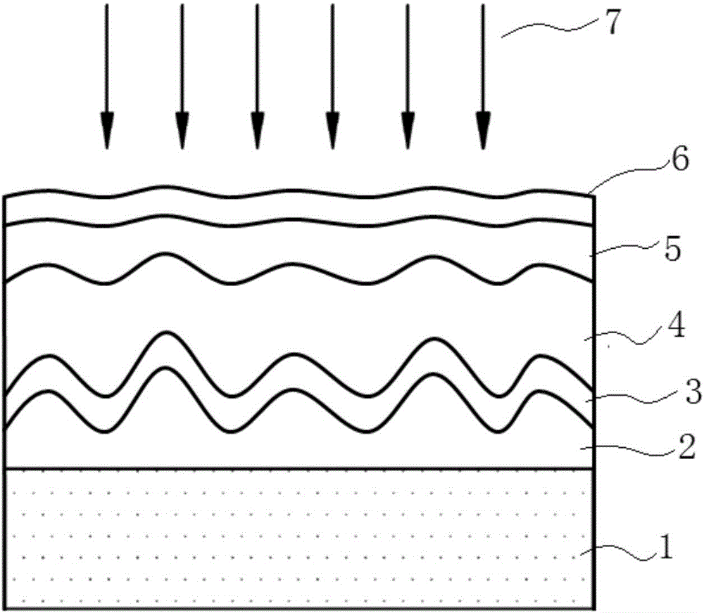
[0033] see figure 1 As shown, a perovskite solar cell based on textured light management structure, including:
[0034] Substrate 1; textured metal back reflection layer 2; electron transport layer 3; perovskite absorption layer 4; hole transport layer 5; transparent conductive front electrode 6, incident sunlight 7 is incident from the direction of the transparent conductive front electrode 6;
[0035] In this embodiment 1, the substrate 1 adopts a stainless steel substrate, the textured metal back reflection layer 2 adopts Ag, the electron transport layer 3 adopts AZO, and the perovskite absorbing layer 4 adopts CH 3 NH 3 PB 3 , the hole transport layer 5 uses Spiro-OMeTAD, and the transparent conductive front electrode 6 uses ITO.
[0036] Its preparation process comprises the following steps:
[0037] Substrate cleaning: first place the stainless steel substrate in a cleaning tank containing electronic cleaning solution for ultrasonic cleaning, the water temperature is...
Embodiment 2
[0044] The difference between this embodiment and embodiment 1 is:
[0045] In step (1), the surface of the stainless steel substrate has a suede topography, and the lateral characteristic size is 1-2 μm, and the suede topography of the base will be transmitted to the subsequent film layer; when depositing the Ag film in the step (2), the temperature is At room temperature, the formed Ag film will not crystallize to form a rough surface, so the feature size of the textured surface is consistent with that of the substrate.
Embodiment 3
[0047] The difference between this embodiment and embodiment 2 is:
[0048] When depositing the Ag film in step (2), use heated sputtering at a temperature of 100-400°C, and the Ag film itself will form a textured surface with a characteristic size of 50-1000nm; in addition, the large-scale textured surface of the substrate It will be conducted to the Ag film, and finally the Ag film will form a suede morphology with a wide distribution of characteristic sizes (50-2000nm).
PUM
 Abstract
Description
Claims
Application Information
 - R&D
- Intellectual Property
- Life Sciences
- Materials
- Tech Scout
- Unparalleled Data Quality
- Higher Quality Content
- 60% Fewer Hallucinations
Browse by: Latest US Patents, China's latest patents, Technical Efficacy Thesaurus, Application Domain, Technology Topic, Popular Technical Reports.
© 2025 PatSnap. All rights reserved.Legal|Privacy policy|Modern Slavery Act Transparency Statement|Sitemap|About US| Contact US: help@patsnap.com

