Antennaless radio frequency electronic tag and its design method
An electronic tag and antenna-less technology, which is applied in computing, computer components, instruments, etc., can solve the problems of narrow bandwidth, reduced reading distance and large size of the tag, and achieve long operating distance, long reading and writing distance, and low cost Effect
- Summary
- Abstract
- Description
- Claims
- Application Information
AI Technical Summary
Problems solved by technology
Method used
Image
Examples
Embodiment 1
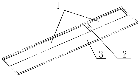
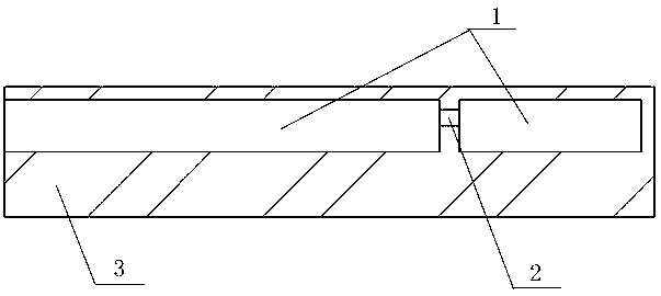
[0035] Embodiment 1 is a capacitive excitation structure such as figure 2 and image 3 As shown, it can be made of materials with higher dielectric constant and low loss. This structure is mainly used in sheet-like planar open metal structures. In this embodiment, the copper on the very thin dielectric board 1 is melted away to form a slot for placing the RFID chip 2 , and the lower end surfaces of the dielectric board 1 and the RFID chip 2 are both placed on the metal copper strip 3 . The excitation structure is placed on the edge of the metal surface where the mode current is small, and attached to the lower surface or the upper surface of the metal surface.
Embodiment 2
[0036] Embodiment 2 is an inductive excitation structure diagram, such as Figure 4 , Figure 5 and Figure 6 , which acts as a coupling coil. In this embodiment, the material 4 with high dielectric constant and low loss can be selected for processing. The metal copper strip 3 surrounds the material 4 in a circle, and the RFID chip 2 is placed at the junction of the two ends of the metal copper strip 3 . The excitation structure is placed at the place where the mode current required to be excited on the metal surface is large, and the direction of the mode magnetic field must pass through the coupling coil vertically to obtain the maximum energy coupling. At the same time, the size of the structure must be adjusted to achieve conjugate matching with the chip. This structure has certain versatility and can be used in a wide range.
Embodiment 3
[0037] Embodiment 3 is a structural diagram of embedding an inductive excitation structure into a metal object, such as Figure 7 As shown, the third excitation structure 5 adopts the structure in Embodiment 2, slots are made at the place where the eigenmode current of the rectangular metal object 6 is the largest, and the third excitation structure 5 is embedded in the metal object to excite the eigenmode current of the metal object In order to realize radio frequency identification, this structure has a certain protective effect on the label, and is concealed and beautiful.
PUM
 Abstract
Description
Claims
Application Information
 - R&D Engineer
- R&D Manager
- IP Professional
- Industry Leading Data Capabilities
- Powerful AI technology
- Patent DNA Extraction
Browse by: Latest US Patents, China's latest patents, Technical Efficacy Thesaurus, Application Domain, Technology Topic, Popular Technical Reports.
© 2024 PatSnap. All rights reserved.Legal|Privacy policy|Modern Slavery Act Transparency Statement|Sitemap|About US| Contact US: help@patsnap.com


