Medium thickness uniformization method of PCB

A medium thickness, PCB board technology, applied in the direction of electrical components, printed circuit liquid treatment, printed circuit manufacturing, etc., can solve the problems that cannot meet the requirements of impedance tolerance, difficult to achieve the production method, etc., to achieve strong operability and applicability, Avoid the effect of medium thickness difference and short process

Active Publication Date: 2016-12-07
GUANGZHOU FASTPRINT CIRCUIT TECH +2
View PDF4 Cites 4 Cited by
  • Summary
  • Abstract
  • Description
  • Claims
  • Application Information

AI Technical Summary

Problems solved by technology

On the other hand, the dielectric thickness tolerance of existing PCB boards generally exceeds 10%, and the contribution to impedance tolerance reaches 5%-6%, which cannot meet the impedance tolerance requirement of 5%.
If the impedance tolerance of 5% is to be met, the dielectric thickness tolerance must be controlled within 7%, but it is difficult to achieve by conventional manufacturing methods

Method used


Image

  • Medium thickness uniformization method of PCB
  • Medium thickness uniformization method of PCB

Examples


Embodiment Construction

[0030] Below, in conjunction with accompanying drawing and specific embodiment, the present invention is described further:

[0031] Such as figure 1 As shown, a method for homogenizing the medium thickness of a PCB comprises the following steps:

[0032] (1) Graphics production, making graphics on the inner copper core board;

[0033] (2) AOI inspection, AOI inspection is performed on the inner layer copper core board that has completed the graphic production;

[0034] (3) Browning treatment, browning treatment is carried out to the inner layer copper core board after AOI detection;

[0035] (4) pre-treatment of solder mask, carry out pre-treatment of solder mask to the inner layer copper core board that has completed the browning treatment;

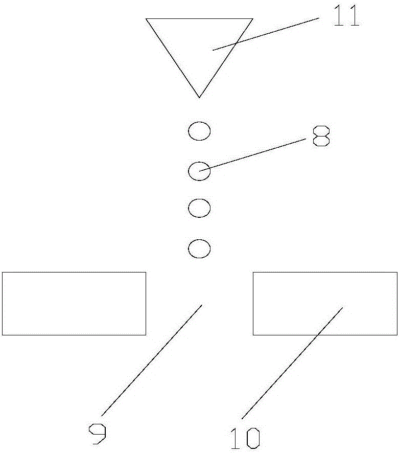
[0036] (5) ink printing, such as figure 2 As shown, ink printing is performed on the inner copper core board that has completed the pre-soldering process by using 3D printing technology, so that the ink 8 completely fills the line ...


PUM


Abstract

The invention discloses a medium thickness uniformization method of a PCB. The method comprises the following steps of 1) pattern preparation in which patterns are prepared in an internal copper core plate; 2) AOI detection in which AOI detection is carried out on the internal copper core board in which the patterns are prepared; 3) brown oxidation in which brown oxidation is carried out on the internal copper core plate after AOI detection; 4) printing-ink printing in which a 3D printing technology is used to print the internal copper core plate after brown oxidation with printing ink so that the printing ink is filled into line gaps in the internal copper core plate and the height of the line gaps filled with the printing ink is the same with that of lines; 5) precuring in which the internal copper core plate printed with the printing ink is precured; and 6) lamination in which the precured internal copper core plate is laminated with prepregs and copper foils. The method can prevent thickness difference of a medium caused by filling of the line gaps effectively, the flow is simple, and the operability is high.

Description

technical field [0001] The invention relates to the technical field of PCB board production, in particular to a method for uniformizing the medium thickness of a PCB board. Background technique [0002] With the development of high-frequency and high-speed signals, PCB impedance control is becoming more and more stringent. At present, the impedance tolerance requirement of 5% has become the mainstream design in some high-speed PCBs. On the other hand, the dielectric thickness tolerance of existing PCB boards generally exceeds 10%, which contributes 5%-6% to the impedance tolerance, and cannot meet the impedance tolerance requirement of 5%. If the impedance tolerance of 5% is to be met, the dielectric thickness tolerance must be controlled within 7%, but it is difficult to achieve it by conventional manufacturing methods. Because there is a height difference between the line gap and the line or the copper surface, during the lamination process, the resin fills the line gap u...

Claims


Application Information

Patent Timeline
Patent Type & Authority Applications(China)
IPC IPC(8): H05K3/00
CPCH05K3/0085H05K2203/013
Inventor 李艳国吴森李华
Owner GUANGZHOU FASTPRINT CIRCUIT TECH
Why Eureka
Try Eureka