Method for eutectic soldering of large substrate on tube shell

A technology of eutectic welding and large substrates, which is applied in the manufacture of electrical components, electric solid devices, semiconductor/solid devices, etc., can solve the problems of long production time period, difficult processing, damage to large substrates and shells, etc., and achieve the goal of manufacturing Simple and cheap, improve the penetration rate, improve the effect of yield

Inactive Publication Date: 2016-12-07
THE 41ST INST OF CHINA ELECTRONICS TECH GRP
View PDF5 Cites 6 Cited by
  • Summary
  • Abstract
  • Description
  • Claims
  • Application Information

AI Technical Summary

Problems solved by technology

But the disadvantage of this method is that on the one hand, after the large substrate is welded on the shell, the void rate is very high, and the void rate of welding is generally very high (over 50%); on the other hand, the preparation of the fixture by this method does not have Applicability, one kind of large substrate needs to correspond to one kind of fixture, the cost is high, and the production time period is long
[0008] It is also disclosed that the welding of the two is achieved by opening the through hole of the microwave substrate and processing the corresponding cylinder of the shell, but the disadvantage of this method is that the large substrate and the shell must be damaged; on the other hand , it is required that the through hole of the large substrate and the cylinder of the shell should be very accurate in position correspondence, and there are difficulties in processing

Method used


Image

  • Method for eutectic soldering of large substrate on tube shell
  • Method for eutectic soldering of large substrate on tube shell
  • Method for eutectic soldering of large substrate on tube shell

Examples


Embodiment Construction

[0029] The specific embodiment of the present invention will be further described below in conjunction with accompanying drawing and specific embodiment:

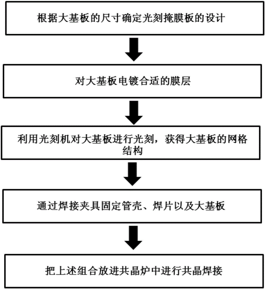
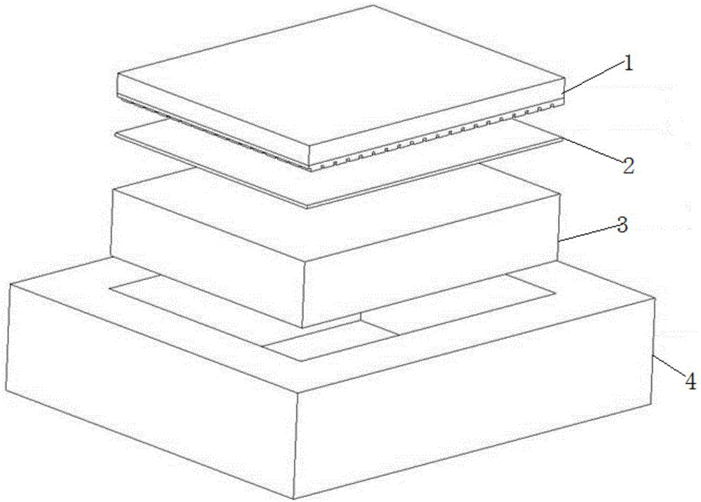
[0030] like Figure 1-4 As shown, a method of eutectically welding a large substrate on a tube shell is carried out in the following order:

[0031] Step 1: Select a suitable photolithography mask according to the specifications of the large substrate; the size of the substrate is generally above 3cm×3cm.

[0032] Step 2: electroplating a film layer on one side of the large substrate;

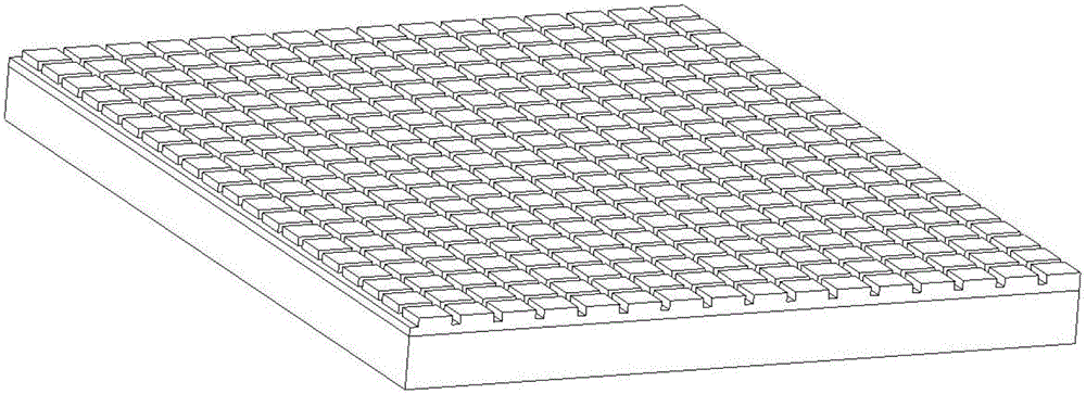
[0033] Step 3: Use a photolithography machine and a photolithography mask to perform photolithography processing on the film layer of the large substrate to obtain a grid-shaped large substrate 1, where the grid is a grid array of 1.9mm×1.9mm, and the grid is The spacing is 0.1mm, the grid is the opaque part in the photolithography mask, and the spacing is the transparent part;

[0034] Step 4: Use the welding jig 4 to fix the shell 3, th...


PUM


Abstract

The invention discloses a method for eutectic soldering of a large substrate on a tube shell, particularly relates to the technical field of welding of the large substrate, and aims at solving the problems that dislocation is easily generated in the welding process of an existing tube shell and the large substrate and the welding voidage is high. The method for eutectic soldering of the large substrate on the tube shell is specifically carried out according to the following sequence: selecting a proper lithography mask according to the specification of the large substrate; electroplating a film at one side of the large substrate; carrying out lithography processing on the film of the large substrate by employing a lithography machine and the lithography mask to obtain a grid-shaped large substrate; fixing the tube shell, a soldering lug and the grid-shaped large substrate through a welding clamp and then carrying out welding in an eutectic furnace; and carrying out welding effect inspection on the welded grid-shaped large substrate.

Description

technical field [0001] The invention belongs to the technical field of welding of large substrates, and in particular relates to a method for eutectic welding of large substrates on a tube shell. Background technique [0002] Vacuum eutectic welding technology is a kind of welding that uses the characteristics of eutectic alloy to realize the welding of chip and substrate, substrate and shell, cover plate and shell. Since eutectic solder pads have better thermal and electrical conductivity than conductive adhesives, and with the increase in the power of microelectronic integrated products, more and more substrates need to be bonded with eutectic soldering instead of conductive adhesives to achieve gold-plated soldering. The interconnection of the tube and shell. [0003] Vacuum eutectic welding belongs to the hot plate heating method, and it can often obtain good penetration rate (the penetration rate can generally reach more than 90%) when welding relatively small componen...

Claims


Application Information

Patent Timeline
Patent Type & Authority Applications(China)
IPC IPC(8): H01L21/60
CPCH01L24/84H01L2224/84136H01L2224/84365
Inventor 宋志明李红伟赵海伦
Owner THE 41ST INST OF CHINA ELECTRONICS TECH GRP
Why Eureka
Try Eureka