Narrow-band infrared detection chip and manufacturing method thereof

A technology of infrared detection and manufacturing method, applied in the field of infrared detection, can solve problems such as high cost, high manufacturing difficulty, insufficient bandwidth, etc., and achieve the effects of high yield, compact and simple system structure, and small volume.

Inactive Publication Date: 2016-12-07
HUAZHONG UNIV OF SCI & TECH
View PDF3 Cites 7 Cited by
  • Summary
  • Abstract
  • Description
  • Claims
  • Application Information

AI Technical Summary

Problems solved by technology

[0004] The invention provides an infrared detection chip that can be used in the field of sensing, which is used to solve the problems of the prior art that the bandwidth is not narrow enough, the manufacturing difficulty is relatively large, and the cost is high, so as to realize the detection target of narrow-band infrared light

Method used


Image

  • Narrow-band infrared detection chip and manufacturing method thereof
  • Narrow-band infrared detection chip and manufacturing method thereof
  • Narrow-band infrared detection chip and manufacturing method thereof

Examples


Embodiment Construction

[0027] In order to make the object, technical solution and advantages of the present invention clearer, the present invention will be further described in detail below in conjunction with the accompanying drawings and embodiments. It should be understood that the specific embodiments described here are only used to explain the present invention, not to limit the present invention. In addition, the technical features involved in the various embodiments of the present invention described below can be combined with each other as long as they do not constitute a conflict with each other.

[0028] The narrow-band infrared detection chip provided by the present invention and its manufacturing method will be described in detail below in conjunction with accompanying drawings 1 to 3 .

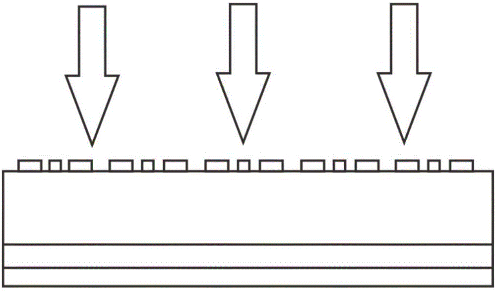
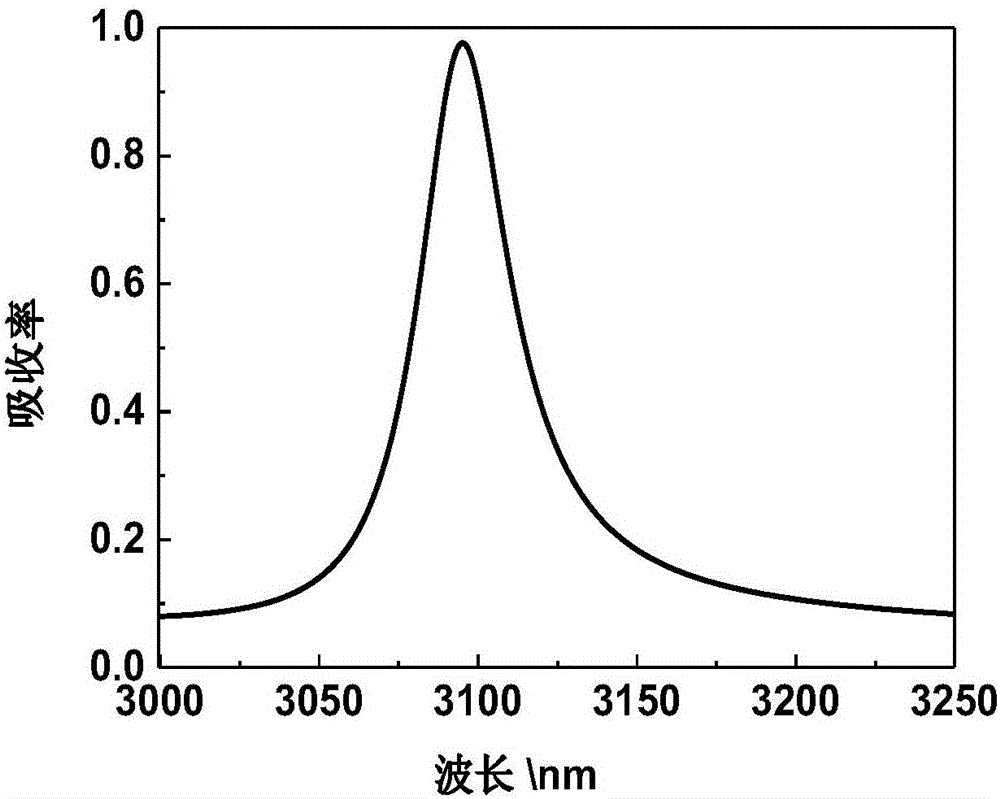
[0029] Such as Figure 1a As shown, the infrared narrowband detection chip of the present invention includes the following main structures, which are sequentially from top to bottom:

[0030] Metal na...


PUM


Abstract

The invention relates to a narrow-band infrared detection chip and a manufacturing method thereof. The manufacturing method comprises the following steps that a monocrystalline wafer is selected and plated with gold with a certain thickness in an evaporation mode; surface deposition of SiO2 with a certain thickness is carried out with PECVD equipment; PMMA exposure glue is smeared in a spinning mode; a nanorod array of a cross structure is designed, the dimension parameter of the nanorod array is precisely controlled, and the designed structure is transferred to the PMMA exposure glue through electronic beam exposure equipment; exposure treatment is carried out, and gold evaporation is carried out with electronic beam evaporation equipment; soaking with a chemical solution is carried out, the PMMA exposure glue is removed, and the nanorod array of the cross structure can be presented on the wafer at the moment. According to the narrow-band infrared detection chip and the manufacturing method thereof, narrow-band infrared detection is achieved by introducing the parameter optimization design of the optical nanometer structure, the manufacturing technology is simple and reliable, and promotion and popularization of the technology are better promoted.

Description

technical field [0001] The invention relates to the technical field of infrared detection, in particular to a design and manufacturing method of a narrow-band detection chip used in the sensing field. Background technique [0002] Infrared detection and sensing is a key technology with wide application. At present, narrow-band absorbing optical antennas and infrared detecting optical antennas have been deeply studied, and great progress has been made. However, no optical antenna has yet achieved narrow-band absorption in the infrared. [0003] A typical structure of this type of chip is the patent document "A Method for Manufacturing Pixel Array of Uncooled Infrared Detection System" (Application No.: 201110302464.4). The proposed manufacturing method has many processes and only has a single function, that is, infrared field imaging , but can not realize the narrowband sensing application. It is unfavorable for realizing the further popularization and application of multi...

Claims


Application Information

Patent Timeline
Patent Type & Authority Applications(China)
IPC IPC(8): G01J3/28G01J3/42B82Y40/00
CPCG01J3/2803B82Y40/00G01J3/42
Inventor 周仑李君宇谈小超杨奥
Owner HUAZHONG UNIV OF SCI & TECH
Why Eureka
Try Eureka