
A high-uniformity impedance plate and its production method

A production method and uniformity technology, applied in the field of high-uniformity impedance plates, can solve problems such as system failure, low dielectric thickness, impedance deviation, etc., and achieve the effect of preventing layer deviation

Active Publication Date: 2019-12-03
广东喜珍电路科技有限公司
View PDF7 Cites 0 Cited by
  • Summary
  • Abstract
  • Description
  • Claims
  • Application Information

AI Technical Summary

Problems solved by technology

[0002] Notebook mainboards need to be equipped with different core board modules, and the two need to ensure that the impedance is within the same range. If there is a difference between the two, it is easy to cause bad phenomena such as the system not turning on.
In PCB production, impedance strips are generally designed outside the unit to simulate the impedance inside the unit, so as to facilitate production control; when the impedance strip is designed on the edge of the board, glue flow is prone to occur due to the height difference of the impedance strip during the pressing process. Resulting in low dielectric thickness and deviation in impedance

Method used


Image

  • A high-uniformity impedance plate and its production method
  • A high-uniformity impedance plate and its production method
  • A high-uniformity impedance plate and its production method

Examples


Embodiment 1

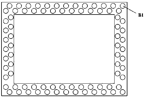
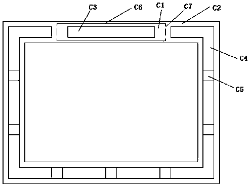
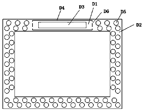
[0034] The present embodiment provides a kind of 12-layer circuit board production method, such as Figure 1-3 shown, including the following steps:

[0035] Lamination;

[0036] drilling;

[0037] Copper plating once;

[0038] outer dry film;

[0039] Secondary copper plating;

[0040] etched copper;

[0041] Solderproof.

[0042] The above pressing process includes

[0043] a. Provide two B-type plates, several C-type plates and D-type plates;

[0044] b. Pre-laminated boards and laminated boards;

[0045] c. Use a PE punching machine to punch PE holes on the edge of the 12-layer circuit board;

[0046] d. Position the 12-layer circuit board through the above-mentioned PE punching holes, and use a fusion machine to perform contact point fusion on the edge of the 12-layer circuit board. The fusion temperature is 260°C and the fusion time is 99s;

[0047] e. Riveting, positioning and riveting the 12-layer circuit board on the riveting machine using the above-mentione...

Embodiment 2

[0059] This embodiment provides a method for producing a 16-layer circuit board, the process of which is consistent with that of Embodiment 1.

[0060] Its pressing process includes

[0061] a. Provide two C-type plates, several B-type plates and D-type plates;

[0062] b. Pre-laminated boards and laminated boards;

[0063] c. Use a PE punching machine to punch PE holes on the edge of the 16-layer circuit board;

[0064] d. Position the 16-layer circuit board through the above-mentioned PE punching holes, and use a fusion machine to perform contact point fusion on the edge of the 16-layer circuit board. The fusion temperature is 235°C and the fusion time is 89s;

[0065] e. Riveting, positioning and riveting the 16-layer circuit board on the riveting machine using the above-mentioned PE punching holes;

[0066] f. Align the fused, riveted and reinforced 16-layer circuit board on the pressing machine for heating and pressing.

[0067] In the present embodiment, the drilling...

Embodiment 3

[0071] This embodiment provides a method for producing a 20-layer circuit board, the process of which is consistent with that of Embodiment 1.

[0072] Its pressing process includes

[0073] a. Provide two C-type plates, several B-type plates and D-type plates;

[0074] b. Pre-laminated boards and laminated boards;

[0075] c. Use a PE punching machine to punch PE holes on the edge of the 20-layer circuit board;

[0076] d. Position the 20-layer circuit board through the above-mentioned PE punching, and use a fusion machine to perform contact point fusion on the edge of the 20-layer circuit board. The fusion temperature is 290°C and the fusion time is 115s;

[0077] e. Riveting, positioning and riveting the 20-layer circuit board on the riveting machine using the above-mentioned PE punching holes;

[0078] f. Heat and press the fused and riveted 20-layer circuit board on the pressing machine.

[0079] In the present embodiment, the drilling process is carried out in the pu...


PUM


Abstract

The invention discloses a high-uniformity impedance board and a production method and a control method thereof. The production method includes a multilayer board lamination procedure which includes steps: a, providing two type-B boards, a plurality of type-C boards and type-D boards; b, performing board pre-stacking and board stacking; c, performing PE punching at edges of a multilayer circuit board; d, fusing; e, riveting and f, laminating. The multilayer circuit board is gradually reinforced by means of fusing and riveting in the lamination procedure and is finally formed by heating lamination, the problem of proneness to layer deflection in lamination of the multilayer circuit board is effectively solved, and the method is especially suitable for production of high multilayer circuit boards. Since compensation of shrinkage and expansion abnormity of inner boards is realized by means of PE punching of the edges of the multilayer circuit board, layer deflection of the inner boards during the lamination procedure is further prevented, product reject ratio is decreased, and precision of the multilayer circuit boards is improved.

Description

technical field [0001] The invention relates to the field of circuit boards, in particular to a high-uniformity impedance board, a production method and a control method thereof. Background technique [0002] Notebook motherboards need to be equipped with different core board modules, and the impedance of the two must be within the same range. If there is a difference between the two, it is easy to cause adverse phenomena such as the system not turning on. In PCB production, impedance strips are generally designed outside the unit to simulate the impedance inside the unit, so as to facilitate production control; when the impedance strip is designed on the edge of the board, glue flow is prone to occur due to the height difference of the impedance strip during the pressing process. As a result, the dielectric thickness is low and the impedance is biased. Especially in the production process of multi-layer circuit boards, the more layers of circuit boards, the more prone to g...

Claims


Application Information

Patent Timeline
Patent Type & Authority Patents(China)
IPC IPC(8): H05K1/02H05K3/46
CPCH05K1/025H05K1/0272H05K1/0298H05K3/46H05K2203/0214
Inventor 付雷黄勇贺波
Owner 广东喜珍电路科技有限公司
Learn More