3d graphene/one-dimensional nanomaterial composite structure field emission cathode and preparation method
A field emission cathode and nano-material technology, which is applied in cold cathode manufacturing, electrode system manufacturing, discharge tube/lamp manufacturing, etc., can solve the problems of not fully utilizing the properties of graphene, achieve good application prospects, increase quantity, Effect of High Electron Mobility
- Summary
- Abstract
- Description
- Claims
- Application Information
AI Technical Summary
Problems solved by technology
Method used
Image
Examples
preparation example Construction
[0031] A preparation method of the above-mentioned 3D graphene / one-dimensional nanomaterial composite structure field emission cathode, comprising the following steps:
[0032] Step 1. Wash the metal foam with a traditional substrate cleaning process, and dry it with nitrogen for later use;
[0033] Step 2, growing graphene on the metal foam after step 1 treatment;
[0034] Step 3, using a deposition method to deposit a one-dimensional nanomaterial seed layer on the substrate with graphene grown after the treatment in step 2;
[0035] Step 4, growing one-dimensional nanomaterials on the substrate treated in Step 3.
[0036] The one-dimensional nanomaterial seed layer is a material seed layer that the one-dimensional nanomaterial has good field emission performance, and ZnO, ZnS, ZnSe, SiC, CuO, MoO can be selected. 2 or AlN with a total thickness of 10-20nm.
[0037] The metal foam cleaning process in step 1 is as follows: first soak in dilute hydrochloric acid for 5-10 min...
Embodiment
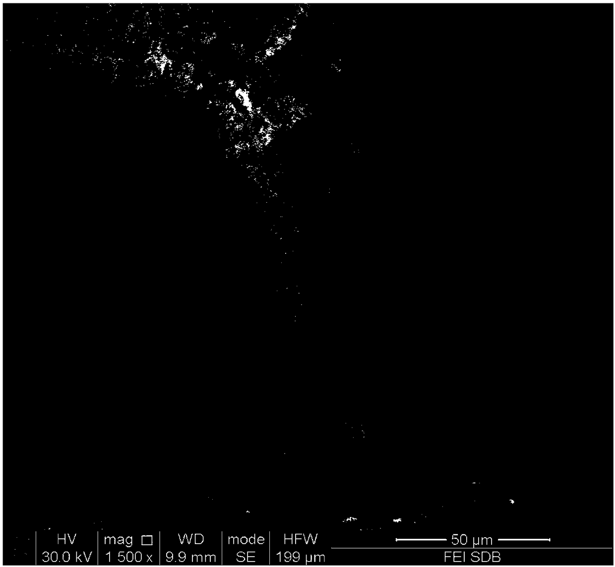
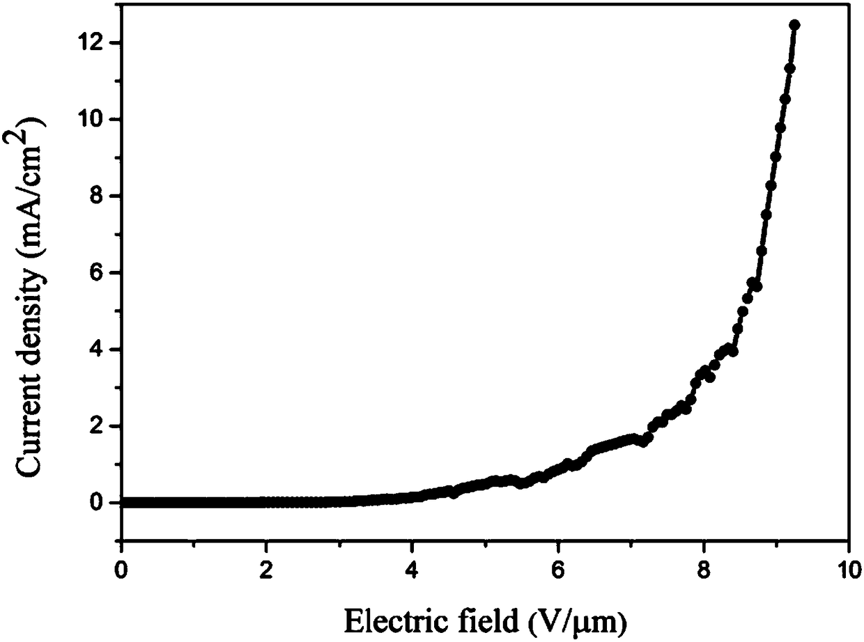
[0039] Cut metal Ni foam 12×10cm (length×width) and clean it, first soak it with dilute hydrochloric acid for 5-10 minutes, then alternately ultrasonicate it with ethanol, acetone, and isopropanol for 10-60 minutes, and blow dry it with nitrogen for later use; put the cleaned metal Ni The foam is placed in a CVD tube furnace to grow 3D graphene; the temperature of the furnace is raised to 930°C, and Ar:H 2 =250: 100sccm annealed for 5 minutes, then 5sccm CH 4 5min; Deposit a zinc oxide seed layer on the grown graphene by atomic layer deposition (ALD), with a deposition thickness of 10-20nm; put the 3D graphene substrate deposited with the zinc oxide seed layer into a zinc oxide growth Zinc oxide nanorod arrays were grown by hydrothermal method in a liquid reaction kettle, the temperature was 90°C, and the time was 3-6h; the growth solution of zinc oxide nanorods was Zn(NO3)2•6H2O (50mM) and hexamethylenetetraammonium ( HMTA, 50mM) mixed solution; finally 80 ℃ vacuum drying fo...
PUM
| Property | Measurement | Unit |
|---|---|---|
| thickness | aaaaa | aaaaa |
| thickness | aaaaa | aaaaa |
Abstract
Description
Claims
Application Information
 - R&D
- Intellectual Property
- Life Sciences
- Materials
- Tech Scout
- Unparalleled Data Quality
- Higher Quality Content
- 60% Fewer Hallucinations
Browse by: Latest US Patents, China's latest patents, Technical Efficacy Thesaurus, Application Domain, Technology Topic, Popular Technical Reports.
© 2025 PatSnap. All rights reserved.Legal|Privacy policy|Modern Slavery Act Transparency Statement|Sitemap|About US| Contact US: help@patsnap.com


