
A pin switch with high stable isolation

A technology with high isolation and high stability, which is applied in the direction of circuits, waveguide devices, electrical components, etc., can solve the problem of not being able to achieve high isolation, stability and consistency of multiple PIN switches, increase the insertion loss index of PIN switches, and reduce the isolation of PIN switches To achieve the effect of strong practicability and application prospects, avoid inconsistency, and fast response speed

Inactive Publication Date: 2018-09-28
SHANGHAI RADIO EQUIP RES INST
View PDF5 Cites 0 Cited by
  • Summary
  • Abstract
  • Description
  • Claims
  • Application Information

AI Technical Summary

Problems solved by technology

[0004] However, in the assembly process of PIN diodes, some errors may occur: 1. Due to the small size of PIN diodes, when cutting microstrip lines, the spacing between microstrip lines cannot be very accurate, and the spacing is often It will be much larger than the width of the PIN diode, causing the interconnected gold wire bonding wire to be too long, thereby reducing the isolation of the PIN switch and increasing the insertion loss index of the PIN switch; 2. The distance between the two PIN diodes The tube spacing cannot be well guaranteed to be 1 / 4 wavelength, so it will also reduce the isolation of the PIN switch
[0005] Due to the errors that may be introduced above, in a multi-channel microwave system, the degree of off-off of the microwave signal of each channel is different, so that the stability and consistency required by the high isolation of multiple PIN switches cannot be achieved.

Method used


Image

  • A pin switch with high stable isolation
  • A pin switch with high stable isolation
  • A pin switch with high stable isolation

Examples


Embodiment Construction

[0021] Combined with Figure 1~ image 3 , a preferred embodiment of the present invention is described in detail.

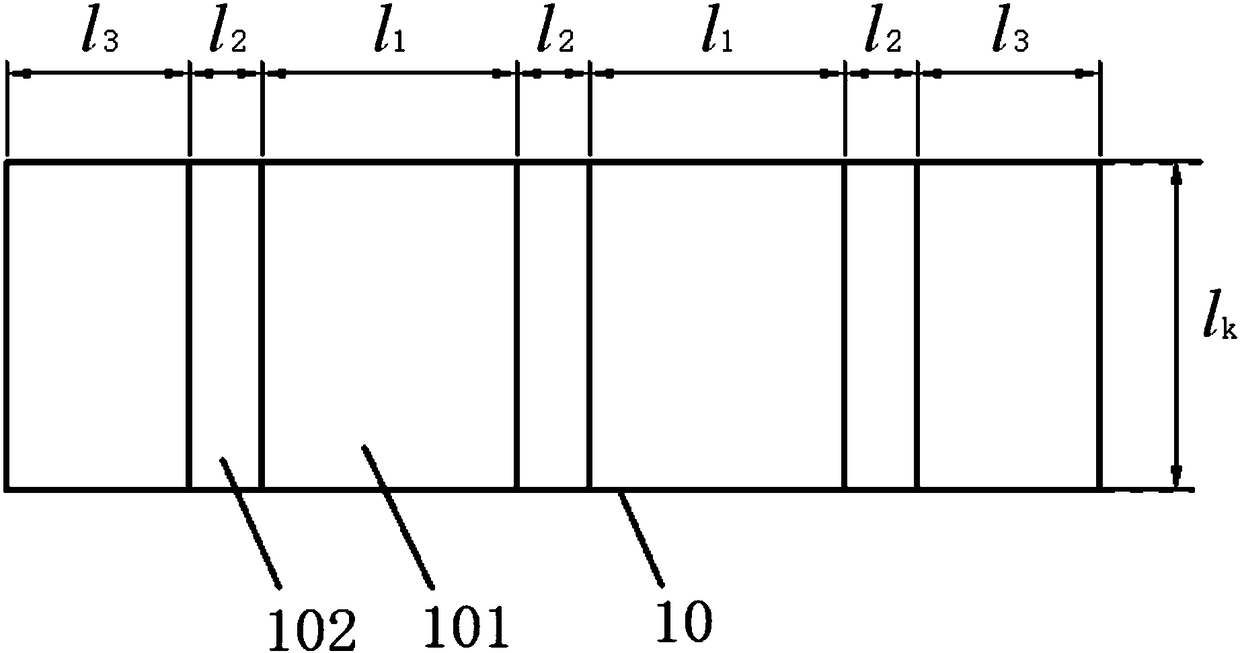
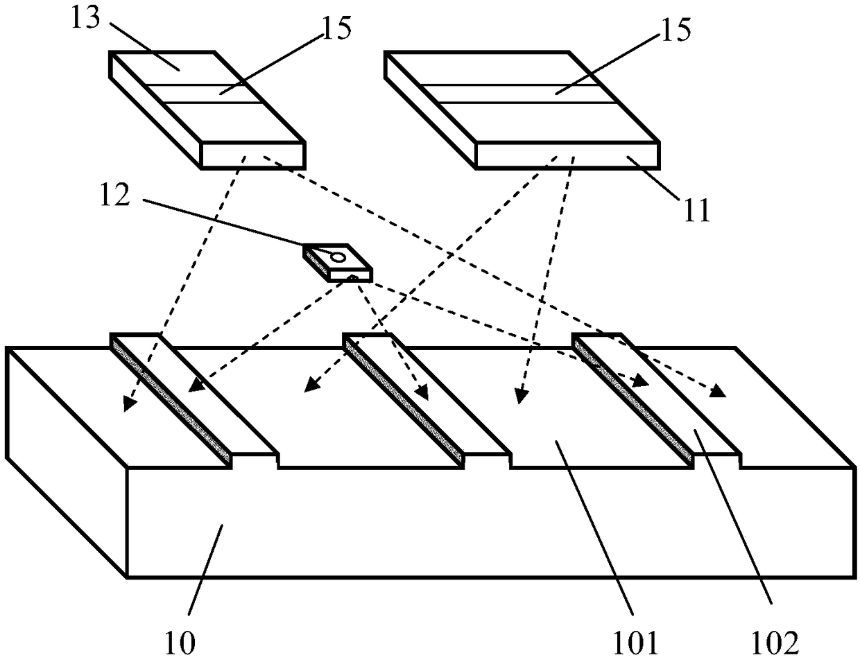
[0022] Such as figure 2 and image 3 As shown, the PIN switch with high stable isolation provided by the present invention includes: a Kovar backing plate 10, on which a plurality of grooves 101 and convex grooves 102 arranged at intervals in sequence are opened on the top surface, and located on the Kovar backing plate 10. Both ends of the backing plate 10 are grooves 101; a plurality of dielectric substrates are respectively arranged on the respective grooves 101, and bonded to the above-mentioned Kovar backing plate 10; each of the dielectric substrates is provided with The microwave signal conduction band 15 is used as a transmission line for transmitting microwave signals; a plurality of PIN diode chips 12 are used to control the on-off of microwave signals to realize the switching function, and are respectively arranged on each convex groove 102 correspo...


PUM


Abstract

The invention relates to a PIN switch with high stable isolation. The PIN switch comprises a kovar backing plate whose upper surface is provided with multiple grooves and protruding grooves with intervals, and the two ends of the kovar backing plate are the grooves. The PIN switch also comprises multiple dielectric substrates which are correspondingly arranged on the grooves and can be bonded to the kovar backing plate. Each of the dielectric substrates is provided with a microwave signal conduction band for transmiting a microwave signal. The PIN switch also comprises multiple PIN diode chips for controlling the on and off of the microwave signal, and the multiple PIN diode chips are corresponding arranged on the protruding grooves and can be bonded to the kovar backing plate. The PIN switch also comprises multiple bonding lines which are bonded with the microwave signal conduction bands connected between every two adjacnet dielectric substrates and the cores of the PIN diode chips, the distance between each two PIN diode chips is 1 / 4 wavelength which indicates the transmission wavelength of the microwave signal on the dielectric substrates. By using a modularization design, the integration use is easy, the degree of isolation is high, the isolation has high stabilization consistency, the PIN switch is used in a multichannel microwave system, and the stabilization consistency of signal turn-off can be realized.

Description

technical field [0001] The invention relates to a PIN switch, in particular to a PIN switch with high and stable isolation, and belongs to the technical field of microwave circuit design. Background technique [0002] In microwave systems, it is often required to control the transmission of microwave signals. The PIN switch uses a PIN diode (a thin layer of low-doped intrinsic Intrinsic semiconductor layer is added between the P semiconductor material and the N semiconductor material to form a P-I-N structure. The diode is a microwave semiconductor control device made of the electrical characteristics of the PIN diode) under different biases, and is widely used in the on-off control of microwave signals. Isolation is a main index of PIN switch, which is used to measure the degree of turning off the microwave signal. [0003] Usually, in order to achieve the high isolation requirements required by the PIN switch, it is necessary to connect multiple PIN diode chips without pa...

Claims


Application Information

Patent Timeline
Patent Type & Authority Patents(China)
IPC IPC(8): H01P1/15
CPCH01P1/15
Inventor 徐晟石磊李雪珺
Owner SHANGHAI RADIO EQUIP RES INST
Learn More