A linear pixel defining layer structure and its preparation method
A pixel-defining layer, pixel-defining technology, applied in semiconductor/solid-state device manufacturing, semiconductor devices, electrical components, etc., can solve problems such as low material utilization rate and complex preparation process
- Summary
- Abstract
- Description
- Claims
- Application Information
AI Technical Summary
Problems solved by technology
Method used
Image
Examples
Embodiment 1
[0029] A method for preparing a linear pixel-defining layer structure is carried out through the following steps:
[0030] A. Deposit a lyophobic insulating layer on the surface of the substrate. In step A, the insulating layer is deposited by spin coating method, and the material of the insulating layer is cytop. The substrate can be ITO or glass or polymer film or other substrates.
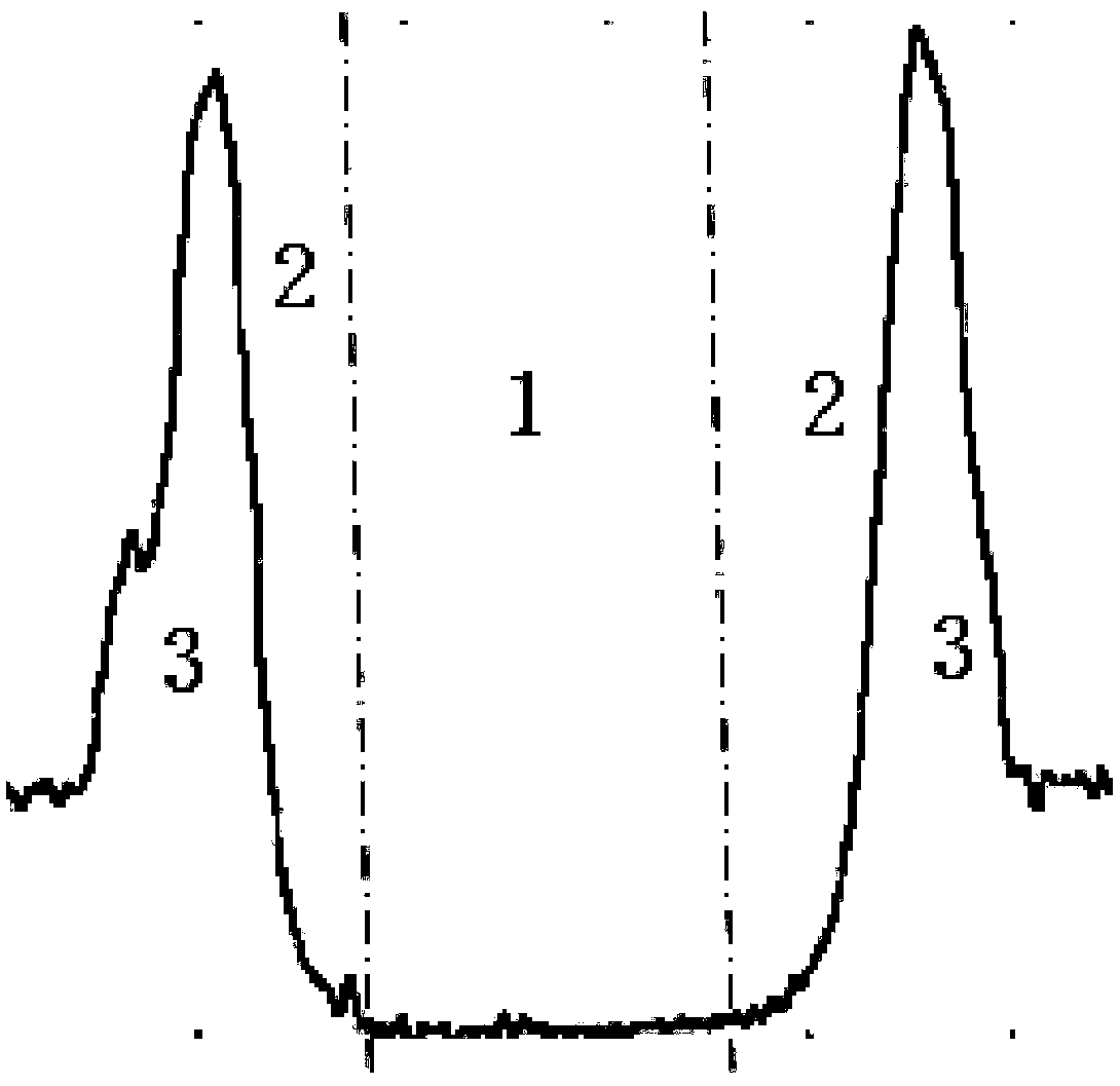
[0031] B. Print a solvent that can dissolve the insulating layer on the surface of the insulating layer. The printed solvent makes the dissolved insulating layer accumulate due to the coffee ring effect to form a pixel wall, and the pixel wall encloses the corresponding pixel limited area. figure 1 It is a schematic diagram of the printed similar structure, the pixel structure is U-shaped, the pixel limited areas 1 and 2 have very little insulating material residue, and 3 is the formed pixel wall.
[0032] Specifically, the inkjet printing method can be used to print the solvent. By adjusting ...
Embodiment 2
[0038] A method for preparing a linear pixel defining layer structure, other features are the same as in Embodiment 1, the difference is that the heat treatment temperature in step D in this embodiment is 190 to 350 degrees Celsius, and the heat treatment time is 6 to 20 minutes. It has been found in practice that the linear pixel defining layer structure prepared by this heat treatment has better performance.
Embodiment 3
[0040] A method for preparing a linear pixel defining layer structure, other features are the same as in Embodiment 1, the difference is that the heat treatment temperature in step D in this embodiment is 200 to 300 degrees Celsius, and the heat treatment time is 6 to 10 minutes. The preparation effect of this process is better.
PUM
 Abstract
Description
Claims
Application Information
 - Generate Ideas
- Intellectual Property
- Life Sciences
- Materials
- Tech Scout
- Unparalleled Data Quality
- Higher Quality Content
- 60% Fewer Hallucinations
Browse by: Latest US Patents, China's latest patents, Technical Efficacy Thesaurus, Application Domain, Technology Topic, Popular Technical Reports.
© 2025 PatSnap. All rights reserved.Legal|Privacy policy|Modern Slavery Act Transparency Statement|Sitemap|About US| Contact US: help@patsnap.com


