Production technology of gold and palladium-plated bonding copper wire for encapsulation

A production process and technology of copper wire, which is applied in the field of production process of gold-plated palladium-bonded copper wire for semiconductor integrated circuit packaging, can solve the problem of unstable electroplating layer of gold-plated palladium-bonded copper wire, easy oxidation of key surface, poor high temperature stability, etc. problem, to achieve the effect of consistent deformation, uniform surface, strong ductility and tensile resistance

Inactive Publication Date: 2016-11-09
上海铭沣科技股份有限公司
View PDF7 Cites 15 Cited by
  • Summary
  • Abstract
  • Description
  • Claims
  • Application Information

AI Technical Summary

Problems solved by technology

[0005] The purpose of the present invention is to invent a production process of gold-plated palladium bonded copper wire for packaging, to overcome the problems of easy oxidation of the existing bonded wire bond surface, poor high temperature stability and wire breakage, and the gold-plated palladium bonded copper wire The electroplating layer is unstable and not resistant to friction, solves the high requirements for the use of gold-plated palladium bonding copper wires and overcomes the technical and cost problems existing in the prior art

Method used


Image

  • Production technology of gold and palladium-plated bonding copper wire for encapsulation

Examples


Embodiment Construction

[0012] The method for manufacturing the gold-plated palladium bonding copper wire proposed by the present invention will be described in detail below through specific implementation methods.

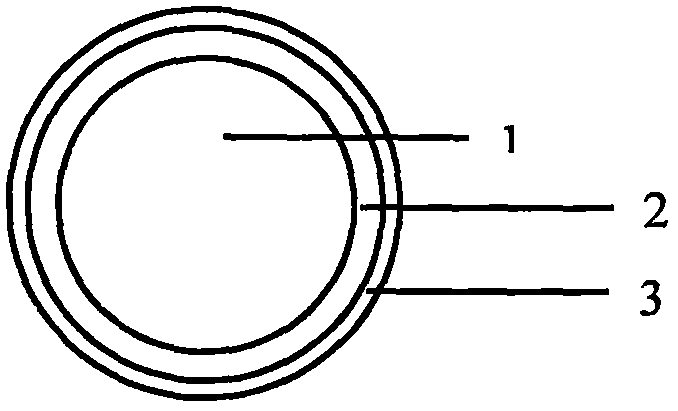
[0013] The gold-plated palladium bonding copper wire proposed in the embodiment of the present invention has a specific structure such as figure 1 As shown, it includes a central copper wire 1, an electroplated palladium layer 2, and an electroplated gold layer 3. Among them, the raw material of the central copper wire 1 is single crystal copper with a purity greater than 99.999%, which is then cast in a high-temperature environment by adding silver, silicon, calcium, aluminum, iron and nickel trace elements; Metal palladium is plated on the surface of the central copper wire by an electroplating process, and the palladium layer can alleviate the problem of oxidation of the central copper wire and the problem of silver drift in the central copper wire, and the binding force between palla...


PUM

PropertyMeasurementUnit
thicknessaaaaaaaaaa
diameteraaaaaaaaaa
thicknessaaaaaaaaaa

Abstract

The invention discloses a production technology of a gold and palladium-plated bonding copper wire for the field of semiconductor integrated circuit encapsulation. The production technology comprises the technological process of carrying out coarse drawing, annealing, palladium layer electroplating, fine drawing, annealing, gold layer electroplating and cleaning on a microelement-added central copper rod treated through a continuous casting technology, so as to prepare the gold and palladium-plated bonding copper wire excellent in physical and chemical property. The technological process is characterized in that only one-time coarse drawing and one-time fine drawing are carried out, and a gold plating technology is carried out after a target wire diameter is achieved through the fine drawing. According to the gold and palladium-plated bonding copper wire produced through the technology, the wire breakage rate during the drawing process is relatively low, the combination property of a palladium-plated layer and a gold-plate layer is good, and the binding reliability and stability of the bonding wire are greatly improved.

Description

technical field [0001] The invention relates to the field of semiconductor integrated circuit packaging, in particular to a production process of gold-plated palladium bonding copper wires for semiconductor integrated circuit packaging. Background technique [0002] Packaging refers to the process of laying out, pasting, fixing and connecting chips on a frame or substrate, leading out terminals and fixing them through plastic packaging to form an overall three-dimensional structure. It not only has the functions of placing, fixing, sealing, enhancing heat dissipation and protecting chips, but also The function of connecting the internal circuit of the chip and the external circuit, and the connection between the internal pad of the chip and the external lead frame is realized through the bonding wire, so there is a high requirement for the conductivity of the bonding wire; in order to make the bonding wire Can be stretched to the required diameter, the metal used must have s...

Claims


Application Information

Patent Timeline
Patent Type & Authority Applications(China)
IPC IPC(8): C25D5/10C25D3/50C21D8/06H01L21/60
CPCC21D8/06C25D3/50C25D5/10H01L24/43H01L2224/43H01L2224/45015H01L2224/45147H01L2224/45572H01L2224/45644H01L2224/45664H01L2924/01204H01L2924/20751H01L2924/20752H01L2924/20753H01L2924/20754H01L2924/20755H01L2924/20756H01L2924/20757H01L2924/01028H01L2924/01013H01L2924/01014H01L2924/0102H01L2924/01026H01L2924/01047H01L2924/01205
Inventor 张志强杨飞马婷婷
Owner 上海铭沣科技股份有限公司
Why Eureka
Try Eureka