Resin eyeglass, lens anti-fog device, preparation method and applications thereof
A resin lens and lens technology, applied in glasses/goggles, optics, instruments, etc., can solve the problems of unsuitable video glasses, poor anti-fog effect, etc., and achieve good anti-reflection effect, low overall resistance, and high conductivity Effect
- Summary
- Abstract
- Description
- Claims
- Application Information
AI Technical Summary
Problems solved by technology
Method used
Image
Examples
Embodiment 1
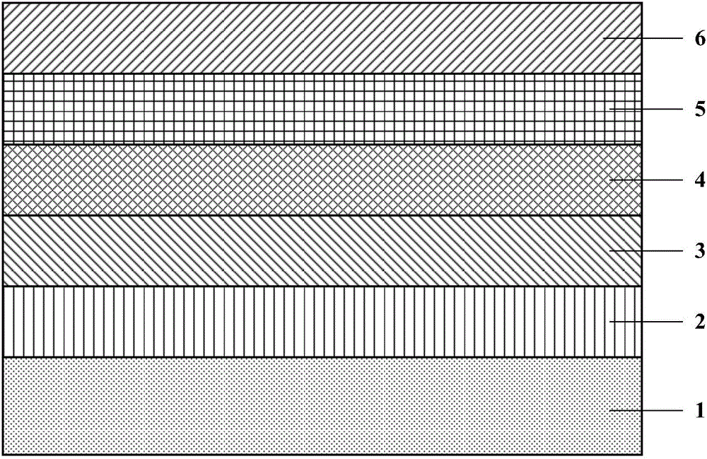
[0045] A kind of resin lens, the schematic diagram of its cross-sectional structure is as follows figure 1 As shown, the resin lens sequentially includes a resin substrate 1, a primer layer 2, a bedding layer 3, a conductive layer 4, an anti-oxidation layer 5 and a protective layer 6 from bottom to top; wherein, the resin substrate is PMMA / PC resin substrate; the bottom layer is a SiO film layer with a thickness of 10nm; the bedding layer is a ZnO film layer with a film thickness of 27.1nm; the conductive layer is an Ag film layer with a film thickness of 6nm; It is a Ti film layer with a thickness of 1nm; the protective layer is Si 3 N 4 The thickness of the film layer is 49.9nm.
[0046] The resin lens is prepared by the following steps:
[0047] (1) After the PMMA / PC resin substrate is cleaned with plasma, it is placed in a magnetron sputtering coating machine, and a pure Si target is fed into oxygen and inert gas for reactive sputtering, and the PMMA / PC composite resin ...
Embodiment 2
[0053] A kind of resin lens, the schematic diagram of its cross-sectional structure is as follows figure 1 As shown, the resin lens sequentially includes a resin substrate 1, a primer layer 2, a bedding layer 3, a conductive layer 4, an anti-oxidation layer 5 and a protective layer 6 from bottom to top; wherein, the resin substrate is PMMA / PC resin substrate; the bottom layer is a SiO film layer, the film thickness is 12.3nm; the bedding layer is a ZnO film layer, the film thickness is 25.6nm; the conductive layer is an Ag film layer, the film thickness is 5nm; anti-oxidation The layer is a Ti film, and the thickness of the film is 1nm; the protective layer is Si 3 N 4 The thickness of the film layer is 67.7nm.
[0054] The resin lens is prepared by the following steps:
[0055] (1) After the PMMA / PC resin substrate is cleaned with plasma, it is placed in a magnetron sputtering coating machine, and a pure Si target is fed into oxygen and inert gas for reactive sputtering, a...
Embodiment 3
[0061] A kind of resin lens, the schematic diagram of its cross-sectional structure is as follows figure 1 As shown, the resin lens sequentially includes a resin substrate 1, a primer layer 2, a bedding layer 3, a conductive layer 4, an anti-oxidation layer 5 and a protective layer 6 from bottom to top; wherein, the resin substrate is PMMA / PC resin substrate; the base layer is a SiO film layer with a thickness of 12nm; the bedding layer is a ZnO film layer with a film thickness of 27.1nm; the conductive layer is an Ag film layer with a film thickness of 10nm; It is a Ti film layer with a thickness of 3nm; the protective layer is Si 3 N 4 The thickness of the film layer is 57.8nm.
[0062] The resin lens is prepared by the following steps:
[0063] (1) After the PMMA / PC resin substrate is cleaned with plasma, it is placed in a magnetron sputtering coating machine, and a pure Si target is fed into oxygen and inert gas for reactive sputtering, and the PMMA / PC composite resin sub...
PUM
| Property | Measurement | Unit |
|---|---|---|
| thickness | aaaaa | aaaaa |
| thickness | aaaaa | aaaaa |
| thickness | aaaaa | aaaaa |
Abstract
Description
Claims
Application Information
 - R&D
- Intellectual Property
- Life Sciences
- Materials
- Tech Scout
- Unparalleled Data Quality
- Higher Quality Content
- 60% Fewer Hallucinations
Browse by: Latest US Patents, China's latest patents, Technical Efficacy Thesaurus, Application Domain, Technology Topic, Popular Technical Reports.
© 2025 PatSnap. All rights reserved.Legal|Privacy policy|Modern Slavery Act Transparency Statement|Sitemap|About US| Contact US: help@patsnap.com


