Making method for thin film transistor array substrate

A technology of thin film transistors and array substrates, which is applied in the field of manufacturing thin film transistor array substrates, can solve the problem of frame width, etc., and achieve the effect of meeting narrow frame, narrow frame and omitting space

Inactive Publication Date: 2016-10-12
WUHAN CHINA STAR OPTOELECTRONICS TECH CO LTD
View PDF13 Cites 10 Cited by
  • Summary
  • Abstract
  • Description
  • Claims
  • Application Information

AI Technical Summary

Problems solved by technology

[0004] The purpose of the present invention is to provide a method for manufacturing a thin film transistor array substrate, so as to solve the technical problem of wide borders caused by the array test circuit in the existing liquid crystal display

Method used


Image

  • Making method for thin film transistor array substrate
  • Making method for thin film transistor array substrate
  • Making method for thin film transistor array substrate

Examples


Embodiment Construction

[0027] The following descriptions of the various embodiments refer to the accompanying drawings to illustrate specific embodiments in which the present invention can be practiced. The directional terms mentioned in the present invention, such as "up", "down", "front", "back", "left", "right", "inside", "outside", "side", etc., are for reference only The orientation of the attached schema. Therefore, the directional terms used are used to illustrate and understand the present invention, but not to limit the present invention.

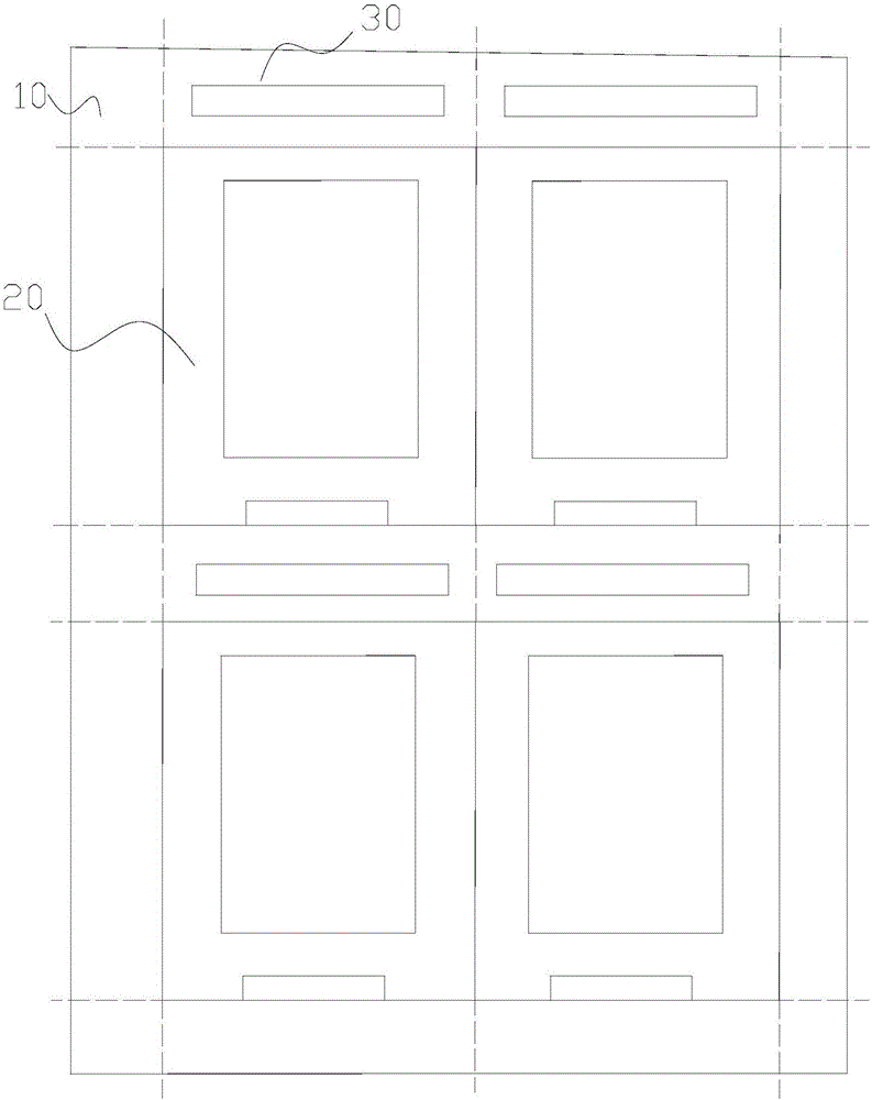
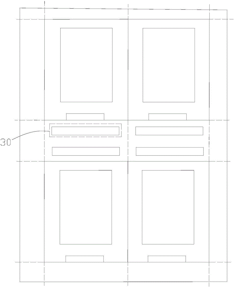
[0028] In the figures, structurally similar units are denoted by the same reference numerals.

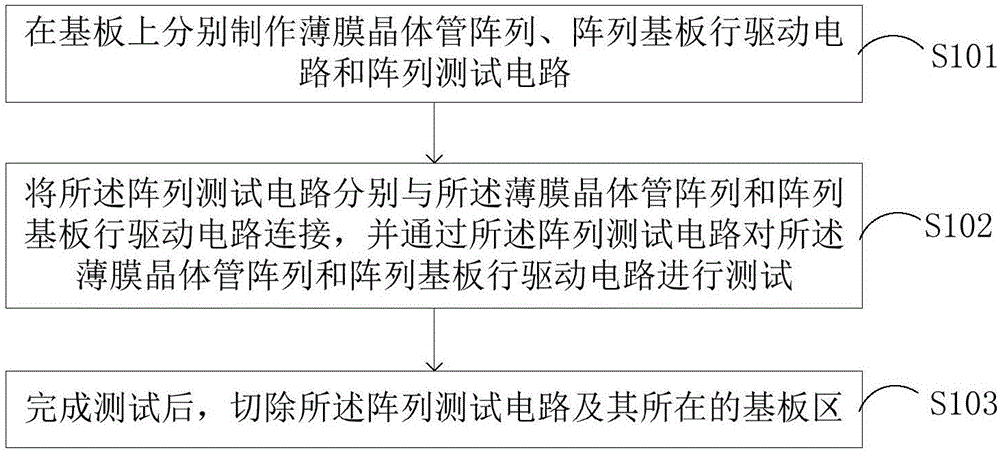
[0029] Please refer to figure 1 , figure 1 It is a flow chart of the manufacturing method of the thin film transistor array substrate of the present invention. In the manufacturing method of the present invention, multiple thin film transistor arrays can be fabricated on a large substrate at the same time, and then cut to form multiple thin film transistor...


PUM


Abstract

The invention provides a making method for a thin film transistor array substrate. The making method includes the steps that a thin film transistor array, an array-substrate row driving circuit and an array test circuit are respectively made on a base substrate; the array test circuit is respectively connected with the thin film transistor array and the array-substrate row driving circuit, and the thin film transistor array and the array-substrate row driving circuit are tested through the array test circuit; after testing is completed, the array test circuit and the substrate area of the array test circuit are cut off. In the making method, before the thin film transistor array substrate is formed through cutting, the prepared thin film transistor array and the array-substrate row driving circuit are tested, and resource wasting caused when a liquid crystal display is made of a poor thin film transistor array substrate is effectively avoided; meanwhile, after the thin film transistor array substrate is tested, the array test circuit is cut off, and therefore a frame of a liquid crystal display can be narrower.

Description

technical field [0001] The invention relates to the technical field of liquid crystal display, in particular to a method for manufacturing a thin film transistor array substrate. Background technique [0002] A thin film transistor liquid crystal display (TFT-LCD) mainly includes a thin film transistor array substrate, a color filter array substrate and a liquid crystal placed between them, wherein the thin film transistor array substrate includes a thin film transistor array and a row driving circuit of the array substrate. At present, when making a thin-film transistor array substrate, an array test circuit will be fabricated on the substrate at the same time, and the thin-film transistor array substrate and the array test circuit will be cut and boxed together to form a liquid crystal display. The array test circuit is used to test the thin-film transistor array. The substrate is tested, and if the TFT array substrate is found to be abnormal, the manufactured liquid cryst...

Claims


Application Information

Patent Timeline
Patent Type & Authority Applications(China)
IPC IPC(8): G02F1/1333G02F1/13
Inventor 洪光辉龚强陈归
Owner WUHAN CHINA STAR OPTOELECTRONICS TECH CO LTD
Why Eureka
Try Eureka