Silicon carbide bipolar junction transistor

A bipolar junction and transistor technology, applied in semiconductor devices, electrical components, circuits, etc., can solve the problems of reducing device current gain and device performance degradation, reducing recombination current, reducing recombination rate, and reducing process complexity. degree of effect

Active Publication Date: 2016-09-28
UNIV OF ELECTRONIC SCI & TECH OF CHINA
View PDF12 Cites 2 Cited by
  • Summary
  • Abstract
  • Description
  • Claims
  • Application Information

AI Technical Summary

Problems solved by technology

[0004] What the present invention aims to solve is that the high interface state density on the surface of the outer base region between the emitter mesa edge and the base ohmic contact of the current SiC BJT will become a recombination center, resulting in a large number of base region minority carriers (electrons) at the interface Recombination produces composite current, which reduces the current gain of the device and causes the degradation of device performance, and provides a silicon carbide bipolar junction transistor

Method used


Image

  • Silicon carbide bipolar junction transistor
  • Silicon carbide bipolar junction transistor
  • Silicon carbide bipolar junction transistor

Examples


Embodiment Construction

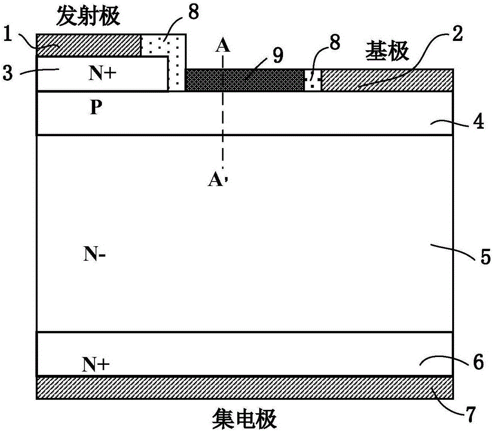
[0017] Below in conjunction with accompanying drawing, describe technical scheme of the present invention in detail:

[0018] In order to increase the current gain of SiC BJT in the prior art, it is necessary to reduce the recombination current on the surface of the outer base region between the edge of the emitter 1 mesa and the base ohmic contact 2. There are three main factors affecting the magnitude of the recombination current:

[0019] 1) Defect concentration at the surface of the exogenous base region;

[0020] 2) The electron concentration at the surface of the exogenous base region;

[0021] 3) The hole concentration at the surface of the extrinsic base region.

[0022] Factor 1 depends on the existing material growth and technology level, and factors 2 and 3 may be affected by the design. The present invention is designed to reduce the recombination current on the surface of the outer base region. In the triode ( figure 2 ), the recombination rate of electron-hol...


PUM

PropertyMeasurementUnit
Thicknessaaaaaaaaaa

Abstract

The invention belongs to the technical field of a high-power semiconductor device, and relates to a silicon carbide bipolar junction transistor. The silicon carbide bipolar junction transistor comprises a collector electrode, an N+ substrate, an N- collector region and a P-type base region, which are stacked up in sequence from the bottom up. One end of the upper surface of the P-type base region is provided with a base electrode, and the other end thereof is provided with an N+ emitter region; the upper surface of the N+ emitter region has an emitter electrode; the upper surface of the P-type base region between the base electrode and the N+ emitter region is provided with an AlN layer; the AlN layer is isolated with the base electrode and the N+ emitter region through heavily-doped layers respectively; and one heavily-doped layer extends to the side away from the base electrode along the upper surface of the N+ emitter region, and is connected with the emitter electrode. The beneficial effects are that, compared with traditional technology, the silicon carbide bipolar junction transistor greatly reduces process complexity, improves qualify rate and reliability of the device and meanwhile, improves current gain of the SiC BJT device.

Description

technical field [0001] The invention belongs to the technical field of high-power semiconductor devices, and relates to a silicon carbide bipolar junction transistor. Background technique [0002] The wide bandgap semiconductor material SiC is an ideal material for preparing high-voltage power electronic devices. Silicon carbide (SiC) bipolar junction transistor (BJT) is one of the important normally-off devices. Advantages. Compared with Si-based transistors, SiC BJT has the advantages of lower turn-on voltage and no secondary breakdown phenomenon; SiC BJT avoids the gate drive problem of normally-on device SiC JFET, and does not have the disadvantage of large conduction loss of SiC IGBT , there is no problem that the working conditions of the SiC MOSFET are limited due to the poor stability of the gate dielectric and the low mobility of the channel. [0003] The existence of SiC / SiO2 high interface state will lead to the instability of the gate dielectric of SiC MOSFET, ...

Claims


Application Information

Patent Timeline
IPC IPC(8): H01L29/06H01L29/16H01L29/732
CPCH01L29/0607H01L29/1608H01L29/732
Inventor 张有润王文郭飞钟晓康刘程嗣刘凯
Owner UNIV OF ELECTRONIC SCI & TECH OF CHINA
Why Eureka
Try Eureka