
Vertical substrate integrated waveguide and vertical connection structure including the waveguide

A technology of substrate integrated waveguide and vertical connection structure, which is applied in the direction of waveguide, waveguide-type devices, circuits, etc., can solve the problems of narrow working bandwidth and difficult integration, and achieve the effect of good transmission bandwidth, compact structure and low loss characteristics

Active Publication Date: 2019-03-05
BEIJING JIAOTONG UNIV
View PDF6 Cites 3 Cited by
  • Summary
  • Abstract
  • Description
  • Claims
  • Application Information

AI Technical Summary

Problems solved by technology

However, due to the waveguide working mode of the substrate-integrated waveguide, using metal vias as the vertical connection structure between substrate-integrated waveguide devices or circuits in different layers will have problems such as difficult integration and narrow operating bandwidth. The gap coupling method is limited to the vertical connection between adjacent layers

Method used


Image

  • Vertical substrate integrated waveguide and vertical connection structure including the waveguide
  • Vertical substrate integrated waveguide and vertical connection structure including the waveguide
  • Vertical substrate integrated waveguide and vertical connection structure including the waveguide

Examples


Embodiment Construction

[0048] In order to illustrate the present invention more clearly, the present invention will be further described below in conjunction with preferred embodiments and accompanying drawings. Similar parts in the figures are denoted by the same reference numerals. Those skilled in the art should understand that the content specifically described below is illustrative rather than restrictive, and should not limit the protection scope of the present invention.

[0049] ·Vertical substrate integrated waveguide

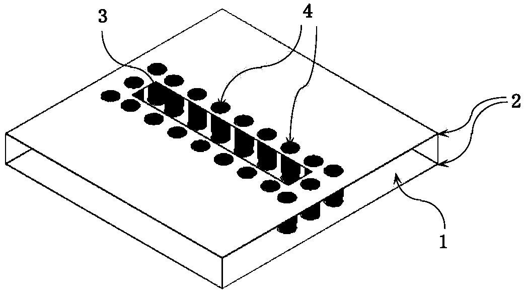
[0050] The vertical substrate integrated waveguide of the present invention includes a dielectric substrate 1 and a metal layer 2 attached to the upper and lower surfaces of the dielectric substrate 1; wherein, the upper and lower surfaces of the dielectric substrate 1 are parallel; There are a plurality of metallized through holes 4 perpendicular to the dielectric substrate 1; the upper and lower surface metal layers 2 cover the metallized through holes 4, and are etched w...


PUM


Abstract

The invention discloses a vertical substrate integrated waveguide and a vertical connection structure comprising the waveguide. The vertical substrate integrated waveguide comprises a dielectric substrate and metal layers, wherein the metal layers are attached to upper and lower surfaces of the dielectric substrate; the upper and lower surfaces of the dielectric substrate are parallel; multiple metalized through holes vertical to the dielectric substrate are formed in the dielectric substrate; the metal layers on the upper and lower surfaces cover the metalized through holes, and are etched with aperture structures which are the same and are corresponding upward and downward; and the metalized through holes are enclosed to form a closed structure along the aperture structures. The vertical substrate integrated waveguide can realize the vertical transmission of electromagnetic energy in the multilayer dielectric substrate.

Description

technical field [0001] The invention relates to an electromagnetic wave transmission structure integrated on a dielectric substrate. More particularly, it relates to a vertical substrate integrated waveguide and a vertical connection structure including the waveguide. Background technique [0002] As the transmission structure of electromagnetic energy, the transmission line is an important part of the microwave and millimeter wave circuit system. As one of the transmission line structures, various metal waveguides have the advantages of low transmission loss and basically no electromagnetic energy leakage in the microwave and millimeter wave frequency bands. However, as the operating frequency increases, the structural size of the metal waveguide will become smaller and smaller, which leads to the continuous improvement of the machining accuracy of the metal waveguide, and the corresponding increase in processing difficulty and cost. On the other hand, a variety of planar...

Claims


Application Information

Patent Timeline
Patent Type & Authority Patents(China)
IPC IPC(8): H01P3/02
CPCH01P3/02
Inventor 李雨键王均宏陈美娥张展李铮
Owner BEIJING JIAOTONG UNIV
Learn More