
Flexible organic semiconductor laser and manufacturing method thereof

An organic semiconductor and laser technology, applied in semiconductor/solid-state device manufacturing, semiconductor devices, electric solid-state devices, etc., can solve the problems of high production cost, inflexible performance, complex production process, etc., and achieve low cost and excellent flexibility. , the effect of low threshold

Inactive Publication Date: 2016-09-21
NANJING UNIV OF POSTS & TELECOMM
View PDF4 Cites 2 Cited by
  • Summary
  • Abstract
  • Description
  • Claims
  • Application Information

AI Technical Summary

Problems solved by technology

Most of the current relatively mature resonators are made of inorganic solid materials. The preparation process is complex, the production cost is high, and they do not have flexible performance. Therefore, it is imperative to manufacture flexible organic lasers at low cost.

Method used


Image

  • Flexible organic semiconductor laser and manufacturing method thereof
  • Flexible organic semiconductor laser and manufacturing method thereof
  • Flexible organic semiconductor laser and manufacturing method thereof

Examples


Embodiment 1

[0015] For the preparation of the flexible substrate, silicone oil and photocuring agent are selected, and the mass ratio is 10:1, and they are stirred evenly; then, the evenly stirred mixed liquid is dropped on the prepared glass sheet, and scraped; put it in a vacuum drying box, Vacuum until there are no bubbles, raise the temperature to 80 degrees Celsius, and take it out after 30 minutes.

[0016] For the preparation of the laser device, spin-coat the flexible substrate prepared above. First, because the contact angle of the prepared substrate is relatively large, it needs to be pre-treated on the surface before it can be spin-coated better. Plasma treatment is selected for 10s. Then spin-coat the isopropanone solution of cellulose acetate in the water-soluble organic interface layer, CA / DAA, 25mg / mL, at a speed of 3000r / min, and finally spin-coat the luminescent layer of PFO, 20mg / mL, at a speed of 2000r / min. By introducing an interface layer, the film-forming property of...

Embodiment 2

[0019] The flexible substrate was prepared according to the method of Example 1.

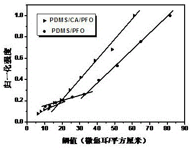
[0020] For the preparation of the laser, the prepared flexible substrate is spin-coated, the surface is pretreated, treated with Plasma for 10s, and then spin-coated with a water-soluble organic interface layer of cellulose acetate in isopropanone solution, CA / DAA, 20mg / mL, rotating speed at 3000r / min, and finally spin-coat the light-emitting layer PFO, 30mg / mL, at a speed of 2000r / min. By changing the concentration of the solution, changing the thickness of the interface modification layer and the organic semiconductor laser gain medium, and observing the change of the laser performance, it is found that the threshold value becomes slightly larger.

Embodiment 3

[0022] The flexible substrate was prepared according to the method of Example 1.

[0023] For the preparation of the laser, the prepared flexible substrate is spin-coated, the surface is pretreated, treated with Plasma for 10s, and then the water-soluble organic interface layer polyelectrolyte (PEs) is spin-coated at 20mg / mL at a speed of 3000r / min, and finally Spin-coat the luminescent layer of PFO, 20mg / mL, and the rotation speed is 2000r / min. By changing the solution and solution concentration of the interface modification layer, observing the effect of changing the solution and thickness of the interface modification layer on the performance of the laser, it is found that the interface modification layer is a water-soluble organic interface layer polyelectrolyte, PEs, water-soluble organic interface layer acetic acid The isopropanone solution of cellulose, CA / DAA, as the interface modification layer, has more stable properties measured.


PUM


Abstract

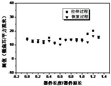
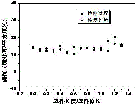
The invention discloses a flexible organic semiconductor laser and a manufacturing method thereof. A device structure comprises an elastic substrateinterface modification layerorganic semiconductor laser gain medium, wherein the elastic substrate is highly elastic plastic, such as Polydimethylsiloxane (PDMS), polyurethane acrylate (PUA), polyving akohol (PVA), etc.; the interface modification layer is an organic polymer interface modification layer filmed by a solution, such as cellulose acetate (CA), polyelectrolytes (PEs), conjugated polyelectrolytes (CPEs), etc.; the organic semiconductor laser gain medium is a laser material possessing optical characteristics. The manufacturing method comprises coating the interface modification layerorganic semiconductor laser gain medium on the elastic substrate through a solution method, the solution method comprising spin coating, spray coating, silk-screen printing, ink-jet printing, etc. The laser prepared according to the method has excellent combination properties, including low light amplification spontaneous radiation threshold (ASE), and sound flexibility (the threshold maintains stable when the laser is bended and distorted randomly or even stretched).

Description

technical field [0001] The invention relates to a flexible organic semiconductor laser and a manufacturing method thereof, belonging to the field of optoelectronic information materials and applications. Background technique [0002] Lasers have extensive and important applications in various fields such as scientific research, medical treatment, military affairs, and engineering construction. With the development of society and the advancement of science and technology, in order to broaden the application range of lasers and enhance their durability, people's demand for new lasers with advantages such as high efficiency, environmental friendliness, flexibility and stretchability is gradually increasing. Due to the many advantages of organic semiconductor materials, the use of organic semiconductor materials will help to develop visible light lasers with high thermal stability, small tunable lasers, optoelectronic integrated devices, especially flexible and even wearable las...

Claims


Application Information

Patent Timeline
Patent Type & Authority Applications(China)
IPC IPC(8): H01L51/42H01L51/46H01L51/48
CPCH10K71/12H10K85/10H10K30/451H10K77/111Y02E10/549
Inventor 赖文勇张静张傲路佩雯
Owner NANJING UNIV OF POSTS & TELECOMM
Learn More