A nanoimprinting device

A technology of nanoimprinting and equipment, applied in the field of nanoimprinting, which can solve the problems of production product impact, high maintenance cost, and large device volume, and achieve the effects of reducing manufacturing requirements, long service life, and strong irradiation intensity

Active Publication Date: 2018-07-03
UNIV OF SCI & TECH OF CHINA
View PDF5 Cites 0 Cited by
  • Summary
  • Abstract
  • Description
  • Claims
  • Application Information

AI Technical Summary

Problems solved by technology

[0004] However, the above-mentioned device has the disadvantages of large volume, short life, high maintenance cost, etc.; in addition, the production material of the light source contains toxic and harmful substances, which can only be installed in the embossing head, and it is easy to produce pollution during the production process, which will also affect the production of products. make an impact

Method used


Image

  • A nanoimprinting device
  • A nanoimprinting device
  • A nanoimprinting device

Examples


Embodiment Construction

[0023] The following will clearly and completely describe the technical solutions in the embodiments of the present invention with reference to the accompanying drawings in the embodiments of the present invention. Obviously, the described embodiments are only some, not all, embodiments of the present invention. Based on the embodiments of the present invention, all other embodiments obtained by persons of ordinary skill in the art without making creative efforts belong to the protection scope of the present invention.

[0024] The core of the invention is to provide a nano imprinting device with no pollution and long service life.

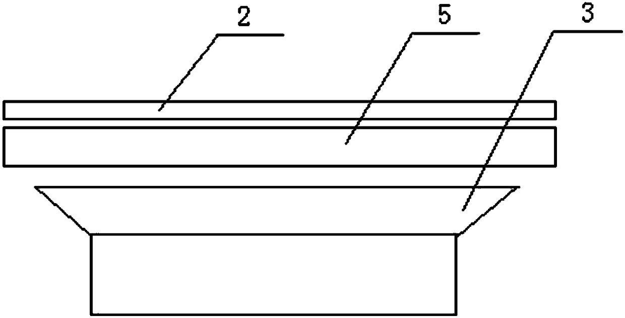
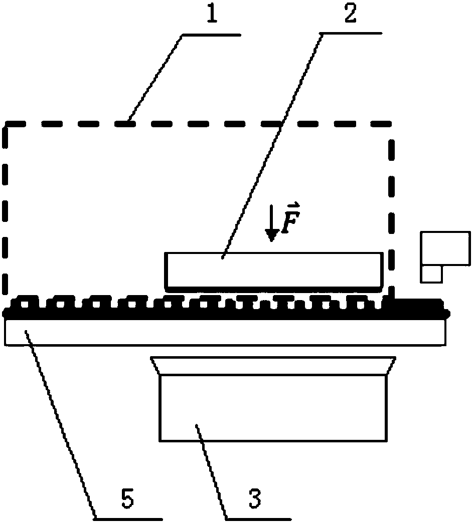
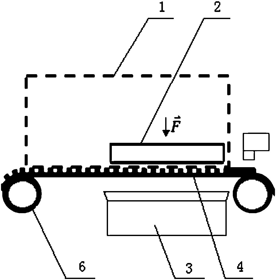
[0025] Please refer to Figure 1 to Figure 3 , figure 1 It is a schematic diagram of a specific embodiment of the nanoimprinting equipment provided by the present invention; figure 2 It is a schematic structural diagram of Embodiment 1 of the nanoimprinting equipment provided by the present invention; image 3 It is a schematic structural diag...


PUM


Abstract

The invention discloses a nano-imprinting device, comprising a nano-imprinting head, a nano-imprinting template is arranged on the nano-imprinting head, a transparent imprinting substrate is arranged under the nano-imprinting template, and a transparent imprinting substrate is arranged under the imprinting substrate. An exposure light source is provided, and the exposure light source is a UV‑LED light source. The UV‑LED light source is safe and non-polluting, and does not produce harmful gases, so the light source can be placed outside the nanoimprint head and below the imprinted substrate. The imprinting template does not need to be made of transparent materials, which reduces the manufacturing requirements of the imprinting template. The use of UV‑LED light sources can also improve the service life of nanoimprinting equipment, because UV‑LED has a long service life and is not affected by the number of opening and closing times, which can reduce production costs and effectively reduce the number of manual maintenance. In addition, UV‑LED is a cold light source that does not generate heat radiation and is suitable for bonding heat-sensitive materials. There is no need to wait for preheating during use, and the irradiation intensity is stronger.

Description

technical field [0001] The invention relates to the technical field of nanoimprinting, and more specifically, relates to a nanoimprinting device. Background technique [0002] Nanoimprint lithography uses the principle of micro-replication of traditional mechanical molds to replace traditional projection lithography including optical, chemical and photochemical reaction mechanisms. Its working principle is to press down the mold to cause the nano photoresist to flow and fill into the characteristic structure on the surface of the mold, then increase the download of the mold to thin the residual layer to the allowable range of the subsequent process, and stop the mold down And curing the nano photoresist. [0003] The curing technologies for curing nano-imprint adhesives in the prior art are all based on mercury lamps, which are electric light sources that use mercury vapor generated during mercury discharge to obtain visible light. Usually, the mercury lamp is arranged ins...

Claims


Application Information

Patent Timeline
Patent Type & Authority Patents(China)
IPC IPC(8): G03F7/20
CPCG03F7/2004
Inventor 王亮谈浩森汪仲儒许凯张博健李晨晖
Owner UNIV OF SCI & TECH OF CHINA
Why Eureka
Try Eureka