Thin film transistor, array substrate, production method of thin film transistor and display device

A technology for thin film transistors and a manufacturing method, which is applied to transistors, semiconductor/solid-state device manufacturing, electric solid-state devices, etc., can solve the problems of low production efficiency, many times of using masks, etc., to simplify the production process, save production costs, The effect of reducing the number of compositions

Active Publication Date: 2016-06-22
BOE TECH GRP CO LTD
View PDF8 Cites 8 Cited by
  • Summary
  • Abstract
  • Description
  • Claims
  • Application Information

AI Technical Summary

Problems solved by technology

[0004] In view of this, an embodiment of the present invention provides a thin film transistor, an array substrate, a manufacturing method thereof, and a display device, so as to solve the existing problems of using masks frequently and low production efficiency when manufacturing thin film transistors.

Method used


Image

  • Thin film transistor, array substrate, production method of thin film transistor and display device
  • Thin film transistor, array substrate, production method of thin film transistor and display device
  • Thin film transistor, array substrate, production method of thin film transistor and display device

Examples


Embodiment Construction

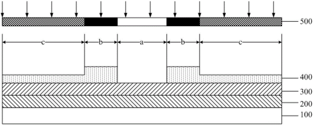
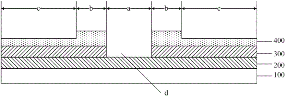
[0045] The specific implementation manners of the thin film transistor, the array substrate, the manufacturing method thereof, and the display device provided by the embodiments of the present invention will be described in detail below with reference to the accompanying drawings.

[0046] The film thicknesses of various layers and the shapes and sizes of the regions in the drawings do not reflect the true proportions of the thin film transistors, but are only intended to schematically illustrate the content of the present invention.

[0047] A method for manufacturing a thin film transistor provided by an embodiment of the present invention includes the following steps: forming patterns of an active layer, source and drain electrodes, and an etch barrier layer on a base substrate through a patterning process, and the etch barrier layer covers The active layer is located between the source and drain electrodes.

[0048] In the manufacturing method of the above-mentioned thin f...


PUM


Abstract

The invention discloses a thin film transistor, an array substrate, a production method of the thin film transistor and a display device. By a one-time patterning process, patterns of an active layer, source and drain electrodes and an etching stopping layer are formed, and the etching stopping layer covers the active layer and is positioned between the source and drain electrodes, i.e. by the one-time patterning process, patterning of three patterns of the active layer, the source and drain electrodes and the etching stopping layer is simultaneously completed. Patterning times in the production process of the thin film transistor are reduced, the production process is simplified, and production cost is saved.

Description

technical field [0001] The invention relates to the field of display technology, in particular to a thin film transistor, an array substrate, a manufacturing method thereof and a display device. Background technique [0002] The 21st century is the era of flat panel display in the field of display. Display devices such as liquid crystal display panels (LCD, Liquid Crystal Display), electroluminescence (EL, electroluminescence) display panels, and electronic paper are well known. These display devices have a thin film transistor (TFT, Thin Film Transistor) that controls the switching of each pixel, and the TFT can be divided into a top-gate TFT and a bottom-gate TFT according to different structures. [0003] Taking the bottom-gate TFT as an example, the manufacturing process is as follows: first, the pattern of the gate is formed on the substrate through a patterning process, and the gate insulating layer is formed on the pattern of the gate; The patterning process forms t...

Claims


Application Information

Patent Timeline
Patent Type & Authority Applications(China)
IPC IPC(8): H01L21/336H01L29/786H01L27/12G02F1/1362
CPCG02F1/1362H01L27/12H01L29/66742H01L29/7869G02F1/1368H01L29/66969H01L27/1288H01L29/78696H01L29/786H01L21/02565H01L21/0273H01L21/425H01L21/47635H01L27/1225H01L29/24H01L29/45
Inventor 宁策杨维
Owner BOE TECH GRP CO LTD
Why Eureka
Try Eureka