


Quick Research
Generate reliable direction feasibility study reports for your R&D in just a few steps.

Technical Q&A
Discover and master advanced knowledge NOW. Basics, ideas, possibilities, all at once.

Find Solutions
As an expert in R&D theories, this can generate solutions to your technical problems instantly.

Evaluate Feasibility
Analyze your overall solution with one click, know your potential R&D risks in advance.

Monitor Landscape
Get weekly tech updates, stay abreast of the latest tech innovations and key insights.
Surface plasma enhancement-based nano laser
A surface plasmon and nano-laser technology, applied in the fields of micro-nano optics and optoelectronics, can solve the problems of high process requirements and complex design structure, and achieve the effect of small size, simple structure and improved performance
- Summary
- Abstract
- Description
- Claims
- Application Information
AI Technical Summary
Problems solved by technology
Method used
Image

Examples
Embodiment example 1
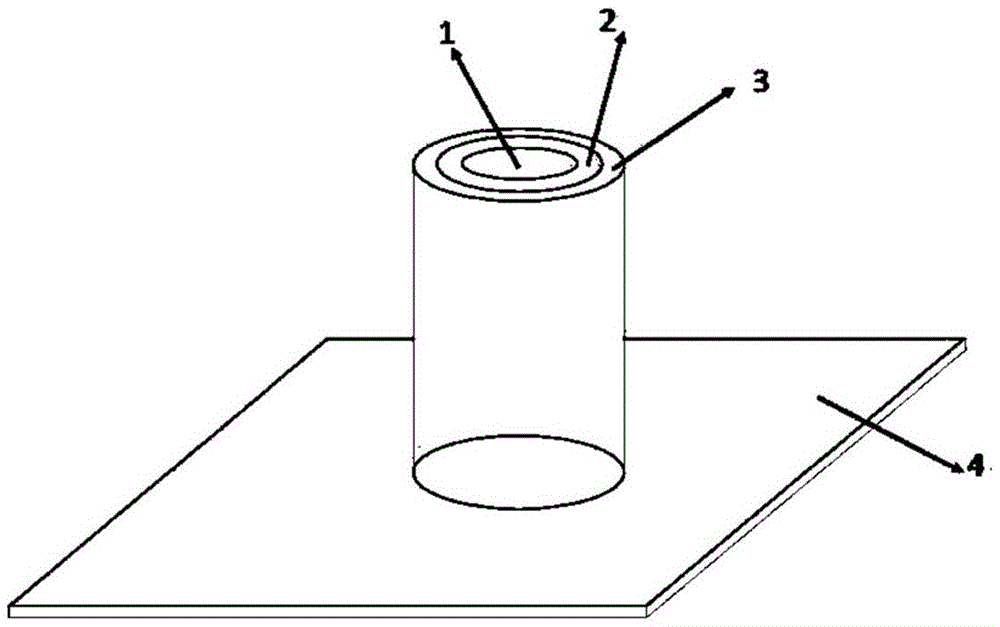
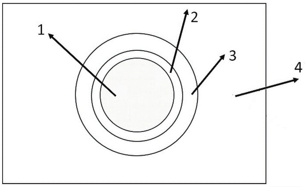
[0020] Implementation Case 1: In this case, the material of the nanowire 1 is zinc oxide as an example, the refractive index is 2.45, the radius is 100 nm, and the length is 2 μm. The insulating dielectric layer 2 is silicon dioxide with a refractive index of 1.468 and a thickness of 10nm; the material of the metal thin film layer 3 is silver with a refractive index of -0.61805i and a thickness of 50nm; the material of the substrate 4 is gallium nitride , with a volume of (length × width × height) 40 μm × 40 μm × 50 μm; this experiment is in a closed and vacuum environment, using an ultra-high vacuum dual ion beam sputtering instrument, and this embodiment uses two high-purity silicon dioxide and Silver is the target material, and by measuring the deposition rate and controlling the deposition deposition time, the deposition thickness ratio of the silicon dioxide film and the silver film is 1:4. The deposition thickness of the silicon dioxide controlled by this embodiment is 10...
Embodiment example 2
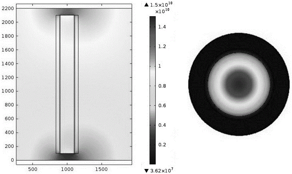
[0022] Example 2: In this case, the zinc oxide nanowires in Example 1 are used, and the same silicon dioxide and silver targets as in Example 1 are used. By measuring the deposition rate and controlling the deposition time, the thickness of the silicon dioxide film is deposited The deposition thickness ratio of the silver film and the silver film is 1:8, the deposition thickness of the silicon dioxide controlled in this embodiment is 5 nm, and the deposition thickness of the silver film is 40 nm. After simulation calculation, with the center of the zinc oxide nanowire as the center, a huge field effect enhancement is produced in the range of 100-105nm, and its maximum field strength is located at 104.5nm, which is 1×10 10 V / m.
[0023] In the background, Zhang Xiang and others disclosed a small semiconductor laser in "Deep Subwavelength Surface Plasmon Lasers" with a power density of up to 131.25Mw cm -2 , the maximum field strength is 36.2V / m; the patent "A Surface Plasma Na...
PUM
| Property | Measurement | Unit |
|---|---|---|
| radius | aaaaa | aaaaa |
| length | aaaaa | aaaaa |
| thickness | aaaaa | aaaaa |
Abstract
Description
Claims
Application Information
 - R&D Engineer
- R&D Manager
- IP Professional
- Industry Leading Data Capabilities
- Powerful AI technology
- Patent DNA Extraction
Browse by: Latest US Patents, China's latest patents, Technical Efficacy Thesaurus, Application Domain, Technology Topic, Popular Technical Reports.
© 2024 PatSnap. All rights reserved.Legal|Privacy policy|Modern Slavery Act Transparency Statement|Sitemap|About US| Contact US: help@patsnap.com