Planar Schottky barrier diode

A Schottky potential and diode technology, which is applied in the field of planar Schottky barrier diodes and silicon planar Schottky barrier diodes, which can solve the inability to meet the requirements of lightning resistance and forward voltage drop, and electrostatic discharge capability. Not meeting the needs and other problems, to achieve the effect of improving the electrostatic discharge capacity, improving the anti-lightning capacity, and improving the forward surge capacity

Inactive Publication Date: 2016-05-04
YANGZHOU GUOYU ELECTRONICS
View PDF4 Cites 2 Cited by
  • Summary
  • Abstract
  • Description
  • Claims
  • Application Information

AI Technical Summary

Problems solved by technology

This type of traditional Schottky diode either meets the requirements for electrostatic discharge capability, but cannot meet the requirements for lightning strike resistance and forward conduction voltage drop; or the lightning strike resistance and forward conduction voltage drop meet the indicators, but the electrostatic discharge capability does not meet the requirements

Method used


Image

  • Planar Schottky barrier diode
  • Planar Schottky barrier diode

Examples


Embodiment Construction

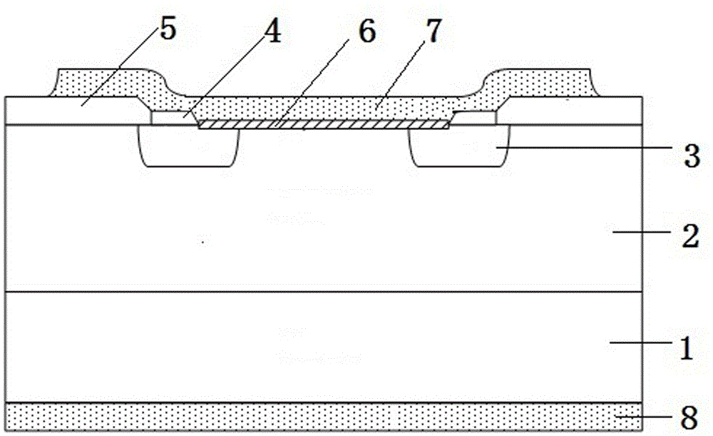
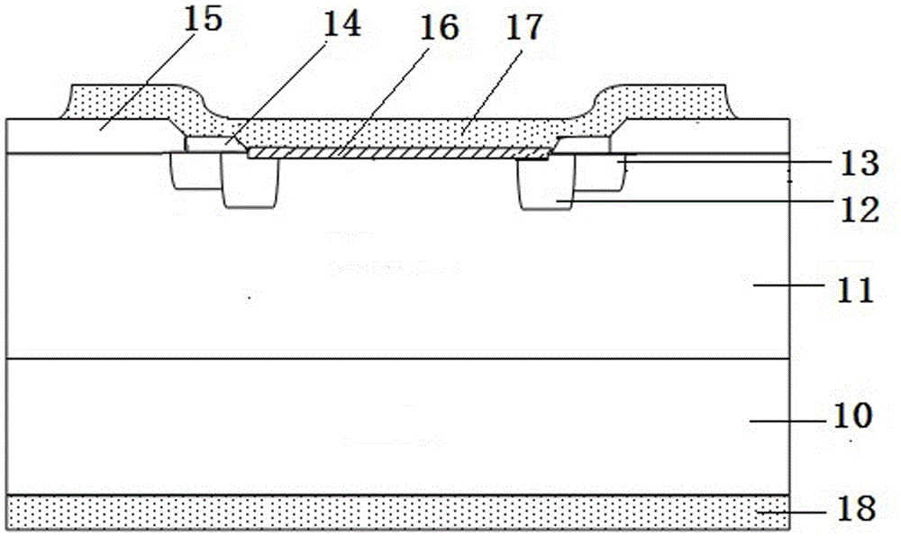
[0011] Aiming at the above-mentioned technical solution, a preferred embodiment is given and described in detail with reference to the drawings. see figure 2 , the planar Schottky barrier diode of the present invention mainly includes an N-type heavily doped silicon substrate, an N-type lightly doped epitaxial layer, a P-type heavily doped ring region, a P-type lightly doped ring region, a thin oxide layer, field oxide layer, Schottky barrier layer, multilayer metal layer, among them.

[0012] The structure of the planar Schottky barrier diode of the present invention is: an N-type heavily doped silicon substrate 10 using an N-type heavily doped silicon chip as a device, and an N-type heavily doped silicon substrate is epitaxially grown on the N-type heavily doped silicon substrate. Lightly doped epitaxial layer 11. The P-type heavily doped ring region 12 is arranged in the N-type lightly doped epitaxial layer, and the P-type lightly doped ring region 13 is arranged in the ...


PUM


Abstract

A planar Schottky barrier diode comprises an N-type heavily-doped silicon substrate, an N-type light-doped epitaxial layer, a P-type heavily-doped loop region, a thin oxide layer, a field oxide layer, a Schottky barrier layer and multiple layers of metal and is characterized in that a P-type light-doped loop region is arranged in the N-type light-doped epitaxial layer outside the P-type heavily-doped loop region, the thin oxide layer is arranged on the P-type heavily-doped loop region and the P-type light-doped loop region, the field oxide layer is arranged on a part of the P-type light-doped loop region and on a part of the N-type light-doped epitaxial layer outside the P-type light-doped loop region, and the Schottky barrier layer is formed on a part of the P-type heavily-doped loop region and on a part of the N-type light-doped epitaxial layer. With the diode disclosed by the invention, the pressure resistant efficiency of the P-type heavily-doped loop region can be effectively improved, the surface field of a Schottkey barrier region can be further enhanced by reducing the junction depth of the P-type heavily-doped loop region, so that the lightning resistance ability of the planar Schottkey barrier is improved, the positive conducted voltage drop can be reduced, and the positive surge capability is improved.

Description

technical field [0001] The invention belongs to the technical field of semiconductor power devices, and is particularly suitable for silicon planar Schottky barrier diodes. More specifically, it relates to a planar Schottky barrier diode that can greatly improve the ability to resist lightning strikes and discharge static electricity. Background technique [0002] At present, power semiconductor devices play an irreplaceable role in the field of power conversion, especially power Schottky diodes, because they have extremely low forward voltage drop, nearly ideal reverse recovery characteristics, and better product consistency. Therefore, it has been widely recognized by the market. At the same time, with the improvement of people's environmental awareness and the sharp reduction of the unit price of solar cells, more and more units and individuals began to favor the purchase of solar cell components for daily production and daily power supply. Due to the changing working en...

Claims


Application Information

Patent Timeline
Patent Type & Authority Applications(China)
IPC IPC(8): H01L29/73
CPCH01L29/7308
Inventor 马文力杨勇谭德喜姚伟明付国振
Owner YANGZHOU GUOYU ELECTRONICS
Why Eureka
Try Eureka