
Board-grade multichip joint test action group (JTAG) chain interconnection structure and method

A multi-chip, board-level technology, applied in the field of JTAG, can solve the problems of slow connection and loading, inconvenient production and design maintenance, and affect the efficiency of production, etc., to achieve easy implementation, convenient testing and production maintenance, and convenient use effect of demand

Active Publication Date: 2016-05-04
GUANGZHOU HUIRUI SITONG INFORMATION SCI & TECH CO LTD
View PDF12 Cites 5 Cited by
  • Summary
  • Abstract
  • Description
  • Claims
  • Application Information

AI Technical Summary

Problems solved by technology

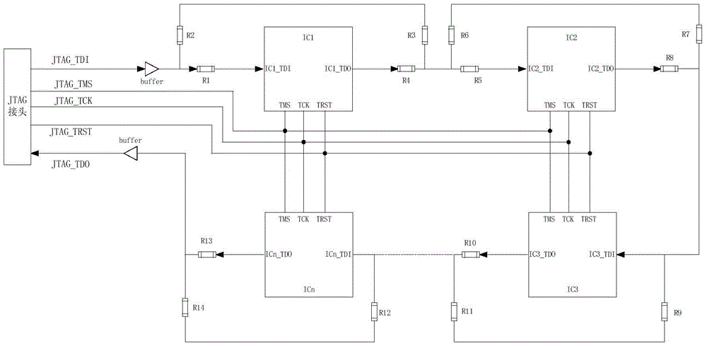
However, there are several disadvantages in this traditional implementation: (1) the operating voltage of electronic devices is various at present, and the devices on the single board have different JTAG interface levels in many cases, so the interface level must be considered. match conversion problem
(2) The isolation method of the hardware jumper resistors, each time the relevant components are bypassed, the corresponding jumper resistors must be manually welded, and the problem must be manually restored after the problem is located, which will bring great inconvenience to the later maintenance.
(3) With the increasing number of devices on the JTAG chain, the longer the chain length, the lower the connection and loading speed, especially for the situation where boundary scan testing is required in production testing, this chaining method will greatly affect production. efficiency
Generally speaking, the above-mentioned JTAG chaining method lacks flexibility and is not convenient for production and design maintenance.

Method used


Image

  • Board-grade multichip joint test action group (JTAG) chain interconnection structure and method
  • Board-grade multichip joint test action group (JTAG) chain interconnection structure and method
  • Board-grade multichip joint test action group (JTAG) chain interconnection structure and method

Examples


Embodiment

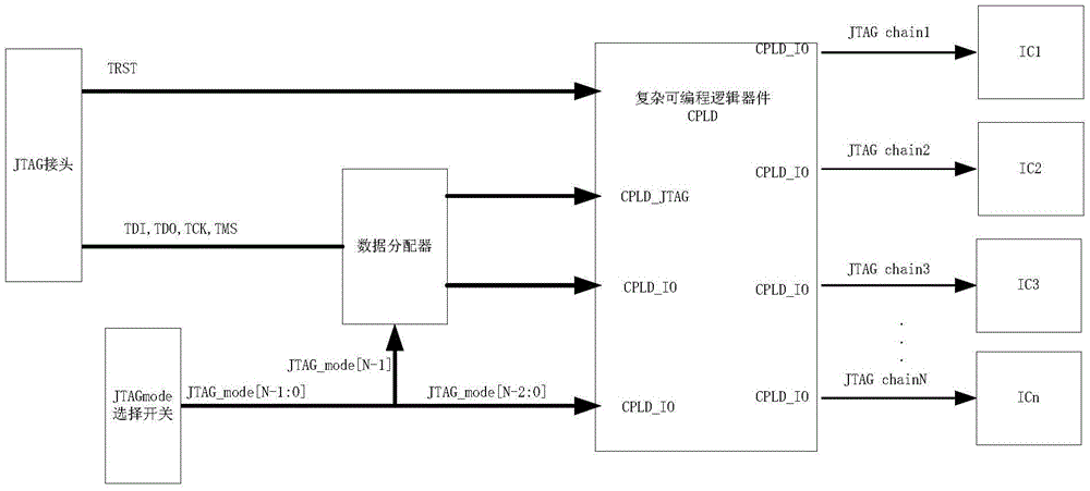
[0035] Such as figure 2 and 4 As shown, the present embodiment discloses a board-level multi-chip JTAG chain interconnection structure, including a JTAG connector and more than one JTAG device, CPLD, data distributor and selection switch; there is a JTAG interface on the CPLD, and the JTAG interface of the CPLD includes a TMS pin, TCK pin, TDI pin, and TDO pin.

[0036] The TMS pin, TCK pin, TDI pin and TDO pin of the JTAG device are respectively connected to the IO port of the CPLD.

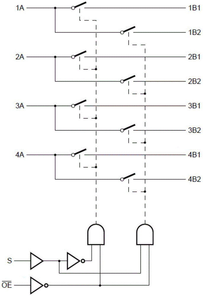
[0037] In this embodiment, the TMS pins, TCK pins, TDI pins and TDO pins of the JTAG connector correspond to the data input terminals connected to the data distributor respectively; The data output end corresponds to the IO port and TMS pin connected to the CPLD respectively, and the data input end of the data distributor connected to the TCK pin of the JTAG connector corresponds to two data output ends respectively corresponding to the IO port and the TCK pin connected to the CPLD; The data...


PUM


Abstract

The invention discloses a board-grade multichip joint test action group (JTAG) chain interconnection structure and method. The structure comprises a JTAG joint, JTAG devices, a complex programmable logic device (CPLD), a data distributer and a selector switch. The TMS pin, the TCK pin, the TDI pin and the TDO pin of the JTAG joint are respectively connected with JTAG interfaces and IO ports of the CPLD through the data distributor; the address signal input end of the data distributor and the IO ports of the CPLD are respectively connected with the selection switch; and the TMS pins, the TCK pins, the TDI pins and the TDO pins of the JTAG devices are respectively connected with the IO ports of the CPLD. According to the invention, chips with the JTAG interfaces on a single board are interconnected by use of the CPLD, such that the function of forming JTAG chains is realized, and different devices on the JTAG chains can be conveniently combined to form chains. The structure and method provided by the invention have the advantages of simple hardware design, high flexibility and greatly facilitated test and production maintenance demands.

Description

technical field [0001] The invention relates to JTAG (JointTestActionGroup, joint test working group), in particular to a board-level multi-chip JTAG chain interconnection structure and method. Background technique [0002] JTAG is an international standard test protocol (IEEE1149.1 compatible), which is used for boundary scan testing of circuits and online programming of programmable chips. The standard JTAG interface is 4 lines, including mode selection line TMS, clock line TCK, data input line TDI and data output line TDO; some JTAG interfaces are 5 lines, including reset line TRST in addition to the aforementioned 4 lines. [0003] In the current electronic hardware system, especially in electronic equipment composed of multiple single boards with complex functions, each single board generally uses multiple highly integrated devices, such as microcontroller units (MCU, MicroControlUnit), digital signal Processor (DSP, DigitalSignalProcessor), field programmable gate arr...

Claims


Application Information

Patent Timeline
IPC IPC(8): G01R31/317
CPCG01R31/31713
Inventor 林伟松
Owner GUANGZHOU HUIRUI SITONG INFORMATION SCI & TECH CO LTD
Learn More