Substrate processing method, substrate processing apparatus, method for manufacturing semiconductor device, and recording medium

一种处理方法、处理容器的技术,应用在半导体/固态器件制造、电气元件、涂层等方向,达到提高制造产能、提高特性的效果

Active Publication Date: 2016-04-20
KOKUSAI DENKI KK +1
View PDF4 Cites 7 Cited by
  • Summary
  • Abstract
  • Description
  • Claims
  • Application Information

AI Technical Summary

Problems solved by technology

[0003] Due to miniaturization in recent years, there is a technical limit to the embedding method by CVD method when embedding oxide into a microstructure, especially when embedding oxide into a vertically deep or laterally narrow void structure.

Method used


Image

  • Substrate processing method, substrate processing apparatus, method for manufacturing semiconductor device, and recording medium
  • Substrate processing method, substrate processing apparatus, method for manufacturing semiconductor device, and recording medium
  • Substrate processing method, substrate processing apparatus, method for manufacturing semiconductor device, and recording medium

Examples


no. 1 approach >

[0044] Hereinafter, a first embodiment which is one of preferred embodiments of the present invention will be described in detail with reference to the drawings.

[0045] (1) Structure of the substrate processing device

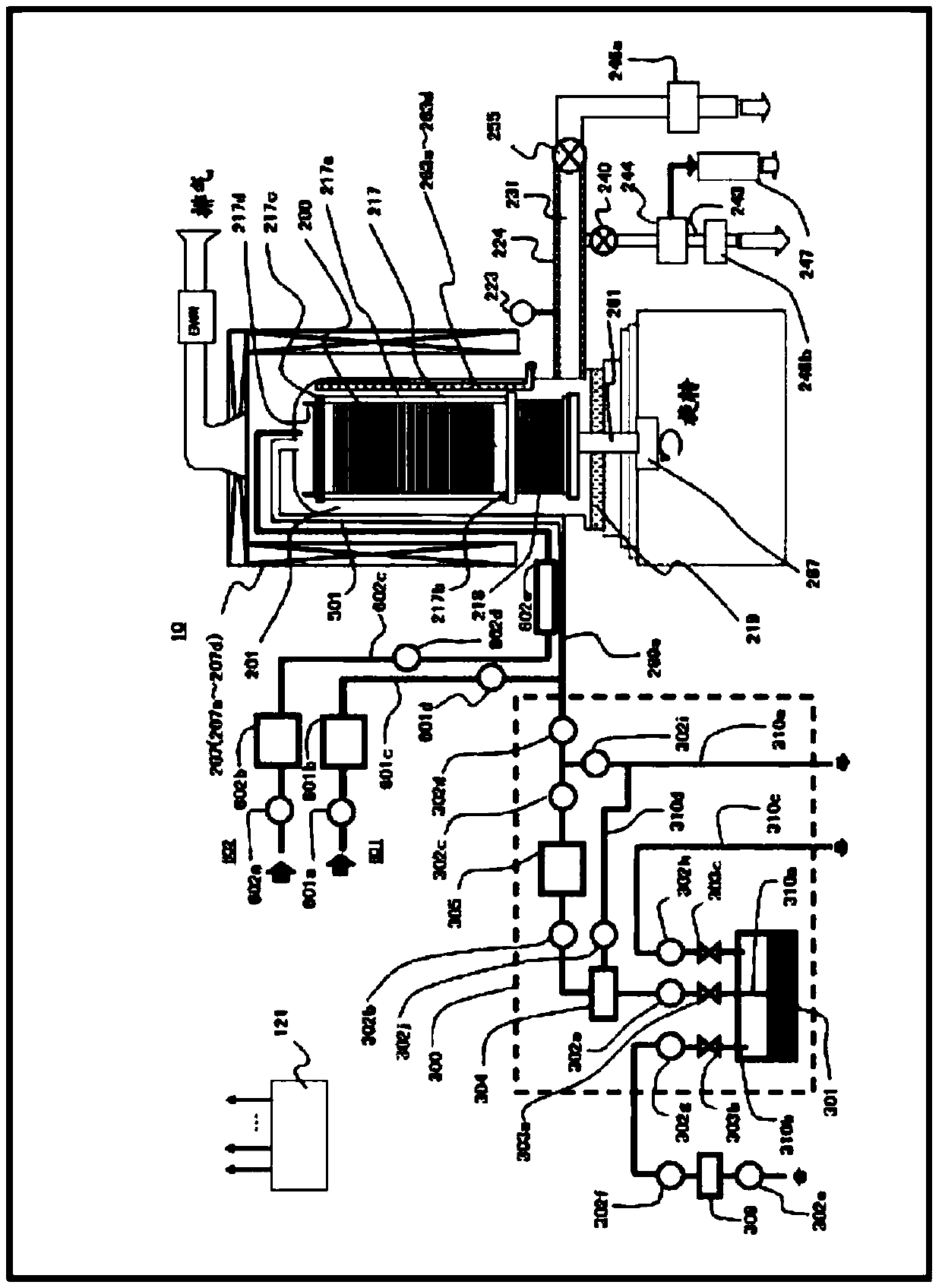
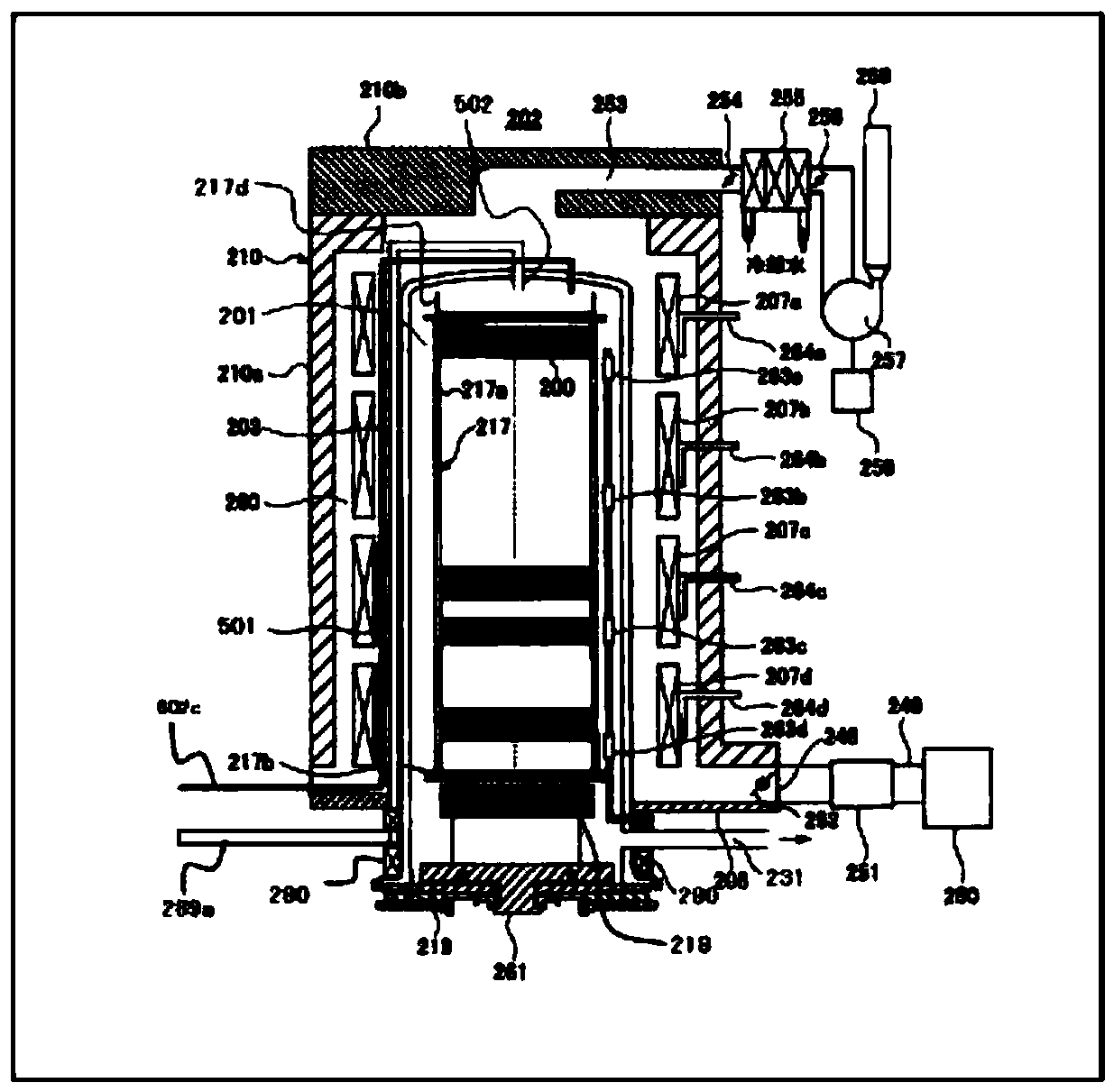
[0046] First, the main use figure 1 and figure 2 The structure of the substrate processing apparatus according to this embodiment will be described. figure 1 It is a schematic configuration diagram of the substrate processing apparatus according to the present embodiment, and shows the processing furnace 202 in vertical section. figure 2 It is a schematic longitudinal sectional view of the processing furnace 202 included in the substrate processing apparatus according to this embodiment.

[0047] (processing container)

[0048] figure 1 As shown, the processing furnace 202 includes a processing container (reaction tube) 203 . The processing container 203 is made of, for example, quartz (SiO 2 ) or silicon carbide (SiC) and other heat-resistant materi...


PUM


Abstract

This substrate processing method comprises: a step wherein a substrate, which is provided with a prebaked film that has a silazane bond, is carried into a process chamber; a modification step wherein the substrate is heated to a first temperature and a processing gas is supplied to the substrate; and a drying step wherein the substrate is heated at a second temperature that is higher than the first temperature but not higher than the temperature of the prebaking.

Description

technical field [0001] The present invention relates to a substrate processing method, a substrate processing device, a manufacturing method of a semiconductor device, and a recording medium. Background technique [0002] With the miniaturization of Large Scale Integrated Circuit (hereinafter referred to as LSI), the processing technology for controlling leakage current interference between transistor elements has increased technical difficulty. LSI element-to-element isolation is performed by forming spaces such as grooves or holes between adjacent elements to be separated on silicon (Si) as a substrate, and depositing an insulator in the spaces. As an insulator, an oxide film is often used, for example, a silicon oxide film (SiO film). The SiO film can be formed by oxidation of the Si substrate itself, chemical vapor deposition (Chemical Vapor Deposition: CVD method), insulator coating method (Spin On Dielectric: SOD method), or the like. [0003] Due to miniaturization ...

Claims


Application Information

Patent Timeline
Patent Type & Authority Applications(China)
IPC IPC(8): H01L21/312H01L21/02H01L21/304H01L21/31
CPCH01L21/67034H01L21/67109H01L21/02126H01L21/02222H01L21/02326H01L21/02337H01L21/02282H01L21/02164C23C16/4481C23C16/46C23C16/52H01L21/02269H01L21/02323
Inventor 奥野正久角田彻立野秀人定田拓也黑川正路
Owner KOKUSAI DENKI KK
Why Eureka
Try Eureka