Metal-insulator-metal capacitor and method for forming same

A technology of insulators and capacitors, applied in capacitors, circuits, electrical components, etc., can solve problems such as poor performance of MIM capacitors, achieve the effect of reducing the thickness and increasing the capacitance value

Active Publication Date: 2016-04-20
SHANGHAI HUAHONG GRACE SEMICON MFG CORP
View PDF4 Cites 12 Cited by
  • Summary
  • Abstract
  • Description
  • Claims
  • Application Information

AI Technical Summary

Problems solved by technology

[0006] The problem solved by the invention is that the performance of the MIM capacitor formed by the prior art is not good

Method used


Image

  • Metal-insulator-metal capacitor and method for forming same
  • Metal-insulator-metal capacitor and method for forming same
  • Metal-insulator-metal capacitor and method for forming same

Examples


Embodiment Construction

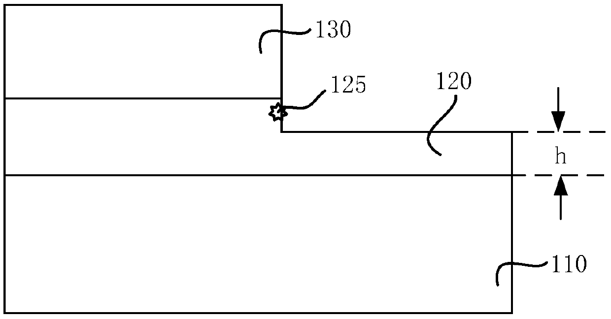
[0028] It can be seen from the background art that the metal-oxide-metal (MIM: Metal-insulator-Metal) capacitor formed in the prior art has poor performance.

[0029] The inventor of the present invention has studied the technology that prior art forms MIM capacitance and finds, as figure 1 As shown, in the prior art, when forming the upper electrode 130 of the MIM capacitor, over-etching is performed to reduce the thickness h of the dielectric layer 120 on the lower electrode 110 . The greater the thickness h of the dielectric layer 120 is, the greater the thickness of the photoresist required for subsequent etching of the lower electrode 110 is, and the etching difficulty increases. However, the more the dielectric layer 120 is etched, the larger the exposed sidewall area of ​​the dielectric layer 120 under the upper electrode 130 is, and etching damage 125 is easily formed on the sidewall during the etching process, resulting in MIM. The time-dependent dielectric breakdown...


PUM


Abstract

The invention provides a metal-insulator-metal (MIM) capacitor and a method for forming the same. The method comprises steps of: providing a substrate, wherein a first conductive layer, a first insulated layer, and a second conductive layer are disposed on the substrate from top to bottom; etching the first conductive layer to form a first electrode which exposes a part of the first insulated layer; forming a second insulated layer covering the top surface and the sidewall of the first electrode and a part of the top surface of the first insulated layer; etching the second insulated layer and the first insulated layer until the second conductive layer is exposed, a sidewall structure is formed by the second insulated layer remaining at the surface of the sidewall of the first electrode and the first insulated layer under the second insulated layer, and a dielectric layer is formed by the first insulated layer under the first electrode; and etching the second conductive layer to form a second electrode. The method for forming the MIM capacitor may decrease etching damage to the dielectric layer in the MIM capacitor.

Description

technical field [0001] The invention relates to the technical field of semiconductors, in particular to a metal-insulator-metal (MIM) capacitor and a forming method thereof. Background technique [0002] Semiconductor devices are used in various electronic devices such as personal computers, mobile phones, digital cameras, and other electronic products. Semiconductor devices are usually manufactured by depositing insulating layers, conductive layers, and semiconductor material layers over a semiconductor substrate, and patterning each material layer using a photolithography process to form circuit components and elements on each material layer. The semiconductor industry reduces the size of semiconductor chips, reduces power consumption, and improves performance by continuously reducing the integration of various electronic components (eg, transistors, diodes, capacitors, resistors, etc.). [0003] Capacitors play the role of decoupling, filtering, resonance, impedance matc...

Claims


Application Information

Patent Timeline
IPC IPC(8): H01L23/64H01L21/02
CPCH01L28/40H01L28/60
Inventor 黄冲李志国董碧云
Owner SHANGHAI HUAHONG GRACE SEMICON MFG CORP
Why Eureka
Try Eureka