Balanced transition circuit of microstrip-substrate integrated waveguide based on probe feeding

A substrate-integrated waveguide and balanced technology, applied in circuits, waveguide-type devices, electrical components, etc., can solve the problems of inconvenient substrate selection, reduced thickness, and large substrate thickness, achieve good common mode suppression effect, and reduce thickness. requirements, the effect of reducing the thickness of the circuit

Active Publication Date: 2015-08-26
江苏嘉兆电子有限公司
View PDF3 Cites 13 Cited by
  • Summary
  • Abstract
  • Description
  • Claims
  • Application Information

AI Technical Summary

Problems solved by technology

[0006] The present invention aims at the traditional probe feeding to realize the transition from the microstrip to the integrated waveguide of the substrate, resulting in a large thickness of the substrate and the inconvenient selection of the substrate caused by strict requirements on the thickness of the substrate. The balanced transition circuit of the electric microstrip to the substrate integrated waveguide realizes the multi-layer heteroplane transition of the differential signal from the microstrip transmission line to the substrate integrated waveguide transmission, simplifies the circuit structure, reduces the thickness, and is easy to manufacture, increasing the Differential mode bandwidth, good common mode suppression effect, strong anti-interference ability and high reliability

Method used


Image

  • Balanced transition circuit of microstrip-substrate integrated waveguide based on probe feeding
  • Balanced transition circuit of microstrip-substrate integrated waveguide based on probe feeding
  • Balanced transition circuit of microstrip-substrate integrated waveguide based on probe feeding

Examples


Embodiment Construction

[0022] The present invention will be further explained below in conjunction with the accompanying drawings and embodiments.

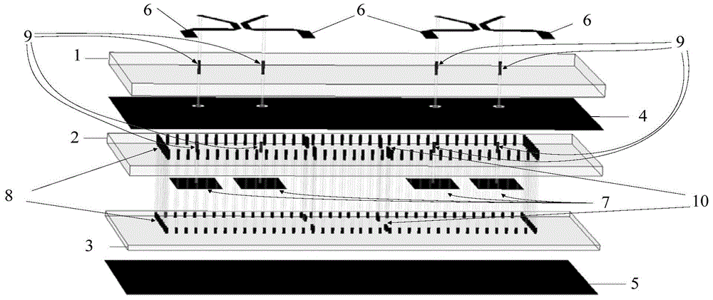
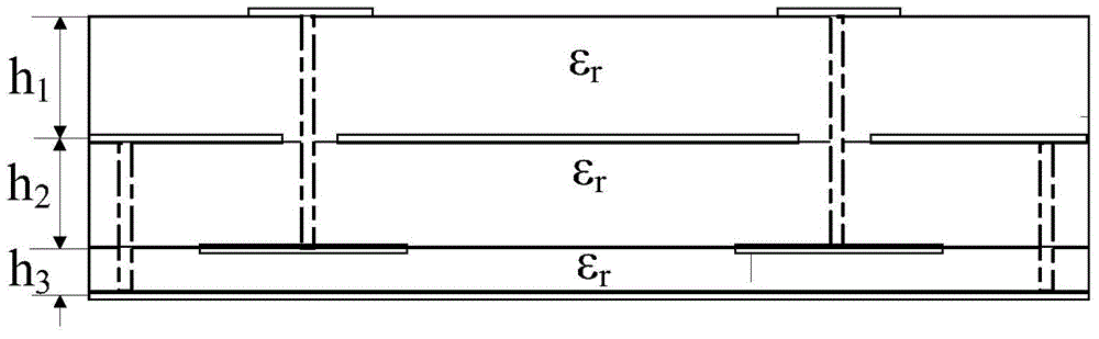
[0023] figure 1 It is a three-dimensional structural schematic diagram of the first embodiment of the balanced transition circuit 100 based on the probe-fed microstrip substrate integrated waveguide of the present invention, as shown in figure 1 As shown, in this embodiment, the balanced transition circuit 100 based on the probe-fed microstrip substrate integrated waveguide includes a first dielectric substrate 1, a second dielectric substrate 2, a third dielectric substrate 3, a first metal Patch 4 , a second metal patch 5 , two input and output transmission line groups 6 and four resonators 7 .

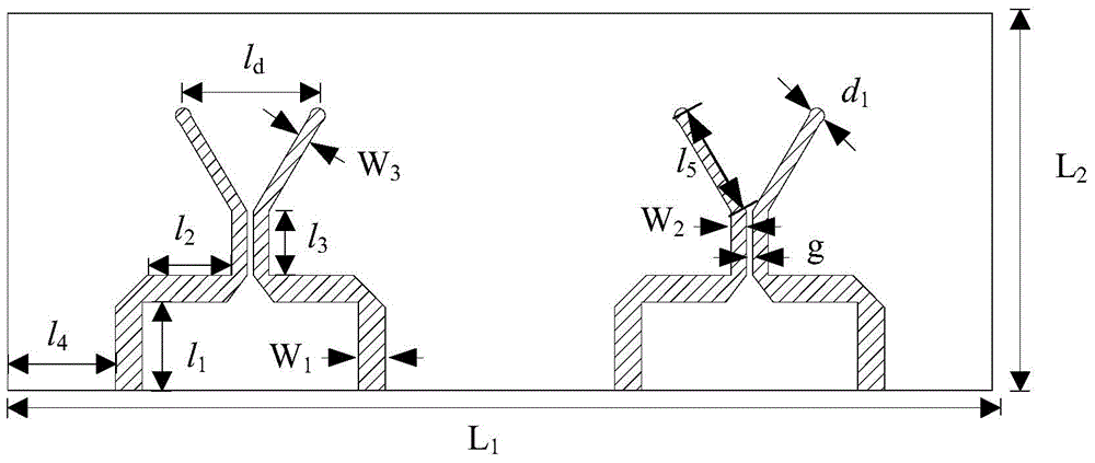
[0024] Wherein, two input / output transmission line groups 6 are arranged symmetrically at both ends of the upper surface of the first dielectric substrate 1, and each input / output transmission line group 6 includes two input / output transmission lines arrange...


PUM


Abstract

The invention discloses a balanced transition circuit of a microstrip-substrate integrated waveguide based on probe feeding. The transition circuit comprises a first dielectric substrate, a second dielectric substrate, a third dielectric substrate, a first metal paster, a second metal paster, four input / output transmission lines and four resonators, wherein first metallized through holes are formed in the second dielectric substrate and the third dielectric substrate to form a substrate integrated waveguide; the first metal paster forms ground of the input / output transmission lines; the resonators are arranged on the upper surface of the third dielectric substrate; the second metal paster forms ground of the substrate integrated waveguide; and four second metallized through holes penetrate through the first dielectric substrate, the first metal paster and the second dielectric substrate. The input / output transmission lines are fed into the substrate integrated waveguide by the second metallized through holes and the resonators at half-wavelength distances, so that a differential signal passes through and a common mode signal is inhibited; and the resonators and the bottom surface of the substrate integrated waveguide arranged below form equivalent capacitance, so that a requirement for the length of a probe is reduced, a requirement for the thickness of the substrate integrated waveguide is reduced, and the thickness of the circuit is reduced.

Description

technical field [0001] The invention relates to the communication field, more specifically, to a balanced transition circuit based on a microstrip substrate integrated waveguide fed by a probe. Background technique [0002] In microwave and millimeter wave commercial and military communication systems, microstrip and substrate-integrated waveguides are two commonly used transmission lines that can efficiently transmit high-frequency signals between various modules. Microstrip transmission lines are commonly used to connect multiple active circuit modules including transistors, monolithic microwave integrated circuits (MMICs), and various surface-mounted components. Since the substrate-integrated waveguide has the characteristics of high Q value, low loss and large power capacity of the metal waveguide, and is easy to process and planarly integrated, it has become the first choice for low-loss transmission lines such as antenna feed networks and high-quality factor filters. ...

Claims


Application Information

Patent Timeline
IPC IPC(8): H01P5/10
Inventor 施金林垄龙陈建新唐慧秦伟周立衡褚慧
Owner 江苏嘉兆电子有限公司
Why Eureka
Try Eureka