


Quick Research
Generate reliable direction feasibility study reports for your R&D in just a few steps.

Technical Q&A
Discover and master advanced knowledge NOW. Basics, ideas, possibilities, all at once.

Find Solutions
As an expert in R&D theories, this can generate solutions to your technical problems instantly.

Evaluate Feasibility
Analyze your overall solution with one click, know your potential R&D risks in advance.

Monitor Landscape
Get weekly tech updates, stay abreast of the latest tech innovations and key insights.
Novel method for modifying GaAs material surface
A gallium arsenide and modification technology, applied in the field of modification of the surface of gallium arsenide material, can solve the problems of contamination, difficult control of process accuracy, easy adhesion, etc., to avoid secondary contamination and good controllability performance and stability, the effect of simplifying process steps
- Summary
- Abstract
- Description
- Claims
- Application Information
AI Technical Summary
Problems solved by technology
Method used
Image


Examples
Embodiment 1
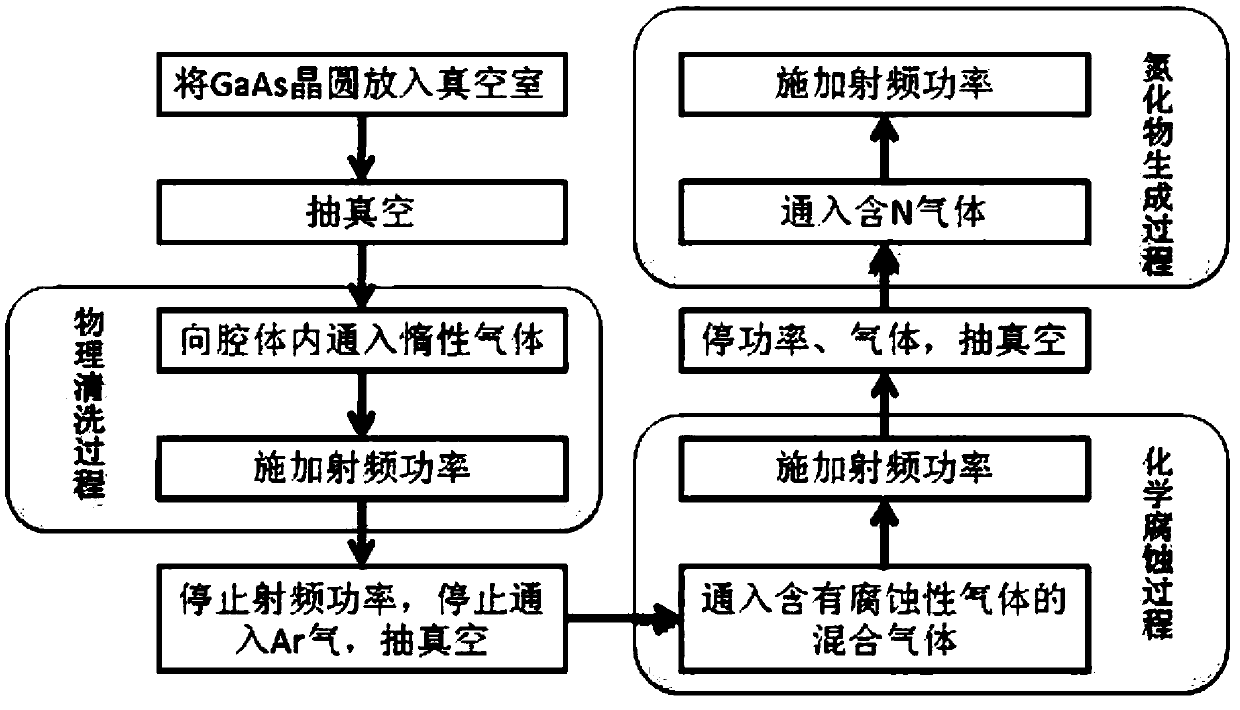
[0027] Step 1. Put the GaAs semiconductor laser bar into the vacuum chamber and pump the vacuum.
[0028] Step 2. Inject 30-100 sccm of Ar gas into the vacuum chamber.
[0029] Step 3. After the air pressure in the vacuum chamber is stabilized at 20-50mtorr, apply a radio frequency power of 10-70W.
[0030] Step 4. After 10-20 minutes, stop applying RF power, stop feeding Ar gas, and vacuum to 2*10^ -4 mtorr.
[0031] Step 5, feed Ar gas and NH into the vacuum chamber 3 Gas (ie corrosive gas) mixed gas, in which Ar gas 20-50sccm, NH 3 Gas 20-70sccm.
[0032] Step 6. After the air pressure in the chamber is stabilized at 20-50mtorr, apply a radio frequency power of 10-50W.
[0033] Step 7. After 5-10 minutes, stop applying RF power, stop feeding Ar gas and NH 3 Gas, vacuum to 2*10^ -4 mtorr.
[0034] Step 8, feed N into the vacuum chamber 2 Gas, the flow rate is 30-100sccm.
[0035] Step 9. After the air pressure in the vacuum chamber is stabilized at 20-50mtorr, appl...
Embodiment 2
[0042] Step 1. Put the GaAs epitaxial wafer into the vacuum chamber and pump the vacuum.
[0043] Step 2. Inject 30-100 sccm of Ar gas into the vacuum chamber.
[0044]Step 3. After the air pressure in the vacuum chamber is stabilized at 20-50mtorr, apply a radio frequency power of 10-70W.
[0045] Step 4. After 10-20 minutes, stop applying RF power, stop feeding Ar gas, and vacuum to 2*10^ -4 mtorr.
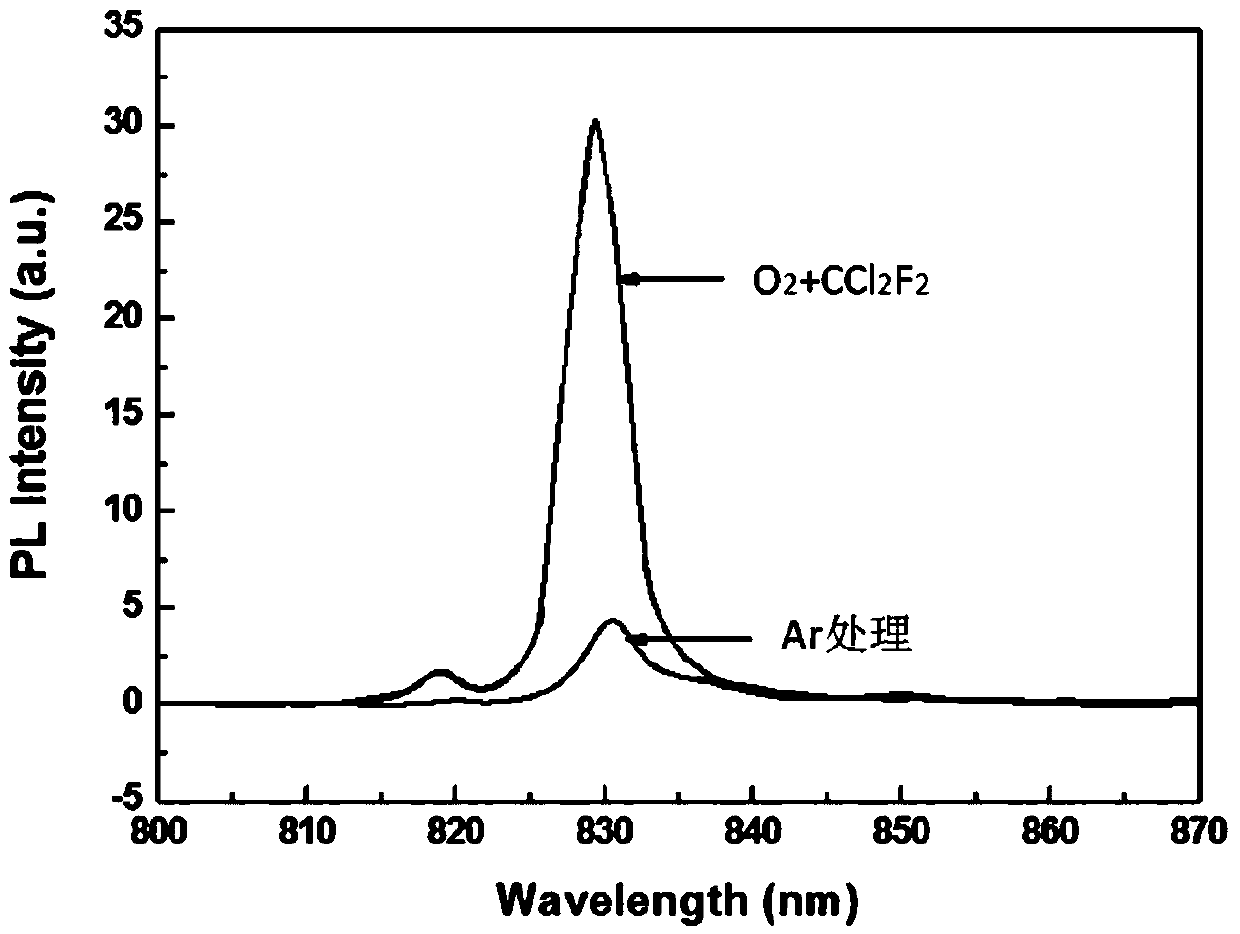
[0046] Step 5, feed oxygen and CCl into the vacuum chamber 2 f 2 Gas (that is, corrosive gas) mixed gas, wherein the oxygen flow range is 10-40sccm, and the CCl2F2 gas flow range is 30-100sccm.
[0047] Step 6. After the air pressure in the chamber is stabilized at 20-50mtorr, apply a radio frequency power of 10-50W.
[0048] Step 7. After 5-10 minutes, stop applying radio frequency power, and stop feeding oxygen and CCl2F2 gas.
[0049] Step 8, feed N into the vacuum chamber 2 Gas, the flow rate is 50-100sccm.
[0050] Step 9. After the air pressure in the vacuum chambe...
PUM
| Property | Measurement | Unit |
|---|---|---|
| electron mobility | aaaaa | aaaaa |
Abstract
Description
Claims
Application Information
 - R&D Engineer
- R&D Manager
- IP Professional
- Industry Leading Data Capabilities
- Powerful AI technology
- Patent DNA Extraction
Browse by: Latest US Patents, China's latest patents, Technical Efficacy Thesaurus, Application Domain, Technology Topic, Popular Technical Reports.
© 2024 PatSnap. All rights reserved.Legal|Privacy policy|Modern Slavery Act Transparency Statement|Sitemap|About US| Contact US: help@patsnap.com