Method for testing weldability of SMD (Surface Mounted Device) product

A solderability and product technology, applied in welding equipment, welding/welding/cutting items, manufacturing tools, etc., can solve the problems of high inspection cost and complicated operation, and achieve the effect of ensuring solderability and reducing inspection cost.

Inactive Publication Date: 2016-04-20
GUILIN STRONG MICROELECTRONICS
View PDF3 Cites 5 Cited by
  • Summary
  • Abstract
  • Description
  • Claims
  • Application Information

AI Technical Summary

Problems solved by technology

At present, the traditional method of testing the solderability of SMD products is: measure the thickness of the tin plating layer of the product, and the thickness is greater than 6 microns, which means good solderability; but the traditional testing method requires large-scale testing equipment, complex operation, high testing cost, and When the equipment is running unstable or the test equipment fails intermittently, it will not be objective and effective to judge the solderability of the product by simply measuring the thickness of the tin plating layer.

Method used


Image

  • Method for testing weldability of SMD (Surface Mounted Device) product

Examples


Embodiment 1

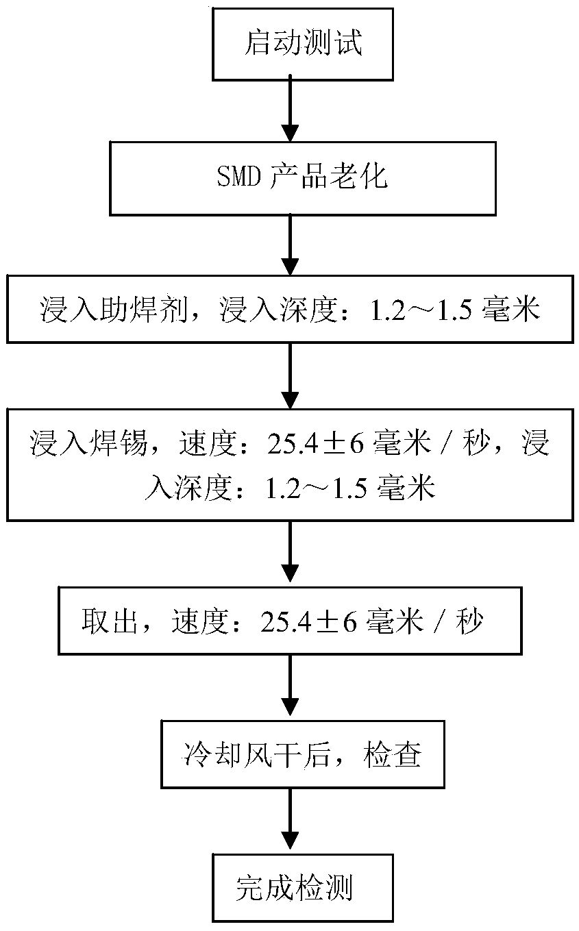
[0017] 1) Freeze the tested SMD product at -8°C for 40 minutes, then take it out and put it in an oven at 150°C for 60 minutes, do this alternately for 3 times, and finally take it out and cool it to room temperature;

[0018] 2) Immerse the surface of all solder ends of the aged SMD product under test into the flux at room temperature. The dipping depth of the pins is 1.5 mm. After keeping for 5 seconds, take it out, and then vertically erect the SMD product under test Clean the filter paper for 3 seconds to remove excess flux and allow to dry for 10 seconds before immersing in solder.

[0019] 3) Turn on the power switch of the tin furnace, set the constant temperature to 230°C; after the temperature of the tin furnace rises to the set temperature, scrape off the scum on the surface of the tin furnace, and put the tested SMD product soaked in flux (plastic package) The front is vertically downward) vertically dipped into the static tin layer at a speed of 25.4 mm / s, the dipp...

Embodiment 2

[0022] 1) Freeze the tested SMD product at -10°C for 40 minutes, then take it out and put it in an oven at 140°C for 80 minutes, do this twice alternately, and finally take it out and cool it to room temperature;

[0023] 2) Immerse the surface of all solder ends of the aged SMD product under test into the flux at room temperature. The dipping depth of the pins is 1.3 mm. After keeping for 5 seconds, take it out, and then vertically stand the SMD product under test on Clean filter paper for 3 seconds to remove excess flux and allow to dry for 10 seconds before immersing in solder, but do not preheat on a solder container.

[0024] 3) Turn on the power switch of the tin furnace, set the constant temperature to 235°C; after the temperature of the tin furnace rises to the set temperature, scrape off the scum on the surface of the tin furnace, and put the tested SMD product soaked in flux (plastic package) The front is vertically downward) vertically dipped into the static tin lay...


PUM


Abstract

The invention discloses a method for testing the weldability of an SMD (Surface Mounted Device) product. After the SMD product is subjected to steps of ageing, immersing in flux, immersing in soldering tin and drying with air, the weldability of the product is judged by observing a covering degree of a tin layer on the surface of the product. The method is simple and direct, expensive detection equipment does not need to be purchased, and thus the weldability of the SMD product is guaranteed while the detection cost is greatly reduced.

Description

technical field [0001] The invention relates to a solderability inspection method, in particular to a method for inspecting the solderability of SMD products. Background technique [0002] In the assembly and welding process of electronic products, if the solderability of circuit boards and components is poor, or the quality or selection of solder paste and flux is poor, it will cause welding problems and directly affect the quality of products. Obvious welding problems include poor wetting, bridging, cracks, tombstones, etc., which will increase the workload of quality inspection personnel and cause a lot of repairs, resulting in a waste of human and financial resources. Invisible welding problems such as false welding, false welding and Poor welding strength, etc., will directly bring about product reliability problems. Solderability test quantitatively evaluates the solderability of the tested samples by testing the solderability of the incoming materials, and directly p...

Claims


Application Information

Patent Timeline
Patent Type & Authority Applications(China)
IPC IPC(8): B23K31/12B23K101/36
CPCB23K31/12B23K2101/36
Inventor 蒋振荣李勇昌彭顺刚黄湖江朱金华
Owner GUILIN STRONG MICROELECTRONICS
Why Eureka
Try Eureka