
Millimeter wave dual-passband filter and design method therefor

A design method and filter technology, applied in waveguide-type devices, circuits, electrical components, etc., can solve the problems of small size, difficult processing and debugging, and difficult to meet the needs of processing level, so as to reduce radiation loss and be conducive to miniaturization. design effect

Active Publication Date: 2016-03-30
超视距(南京)科技有限责任公司
View PDF4 Cites 7 Cited by
  • Summary
  • Abstract
  • Description
  • Claims
  • Application Information

AI Technical Summary

Problems solved by technology

The traditional metal waveguide structure has the advantages of high Q value, large power capacity, and low loss, but it has disadvantages such as large volume, difficult processing and debugging, and difficulty in integrating with the plane; the stripline structure is small in size and flexible in layout, but its open The coaxial structure introduces a large radiation loss in the millimeter wave frequency band, which is not suitable for millimeter wave band applications; the coaxial structure has a high Q value and a large power capacity, but in the millimeter wave frequency band, its size is too small, and the existing processing level is not easy to meet the demand. , and it is also difficult to integrate with planar circuits

Method used


Image

  • Millimeter wave dual-passband filter and design method therefor
  • Millimeter wave dual-passband filter and design method therefor
  • Millimeter wave dual-passband filter and design method therefor

Examples


Embodiment Construction

[0034] The specific embodiments of the present invention are described below so that those skilled in the art can understand the present invention, but it should be clear that the present invention is not limited to the scope of the specific embodiments. For those of ordinary skill in the art, as long as various changes Within the spirit and scope of the present invention defined and determined by the appended claims, these changes are obvious, and all inventions and creations using the concept of the present invention are included in the protection list.

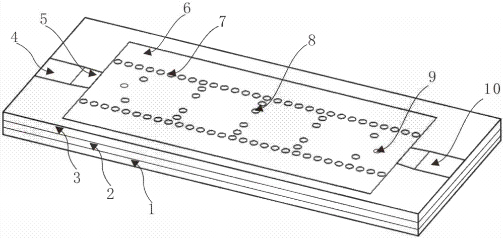
[0035] Such as figure 1 As shown, the millimeter-wave dual-passband filter includes a first PCB board 3 and a second PCB board 1 bonded together by an adhesive layer 2, and an SIW disposed on the first PCB board 3 and the second PCB board 1 The filter and the lower sideband filter arranged on the lower surface of the first PCB board 3 .

[0036] Among them, the first PCB board 3 adopts TaconicTLY-5, its dielectric constant...


PUM

PropertyMeasurementUnit
Thicknessaaaaaaaaaa

Abstract

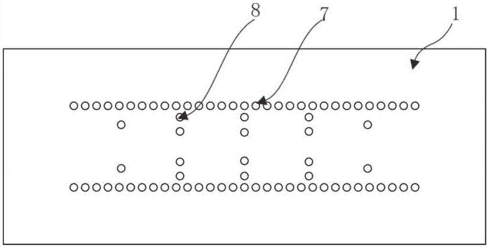
The invention discloses a millimeter wave dual-passband filter and a design method therefor. The millimeter wave dual-passband filter comprises a first PCB and a second PCB that are adhered to each other through a bonding layer, an SIW filter arranged on the first PCB and the second PCB, and a lower sideband filter arranged on the lower surface of the first PCB; the SIW filter comprises a copper coating layer arranged on the upper surface of the first PCB, a copper coating layer arranged on the lower surface of the second PCB, and a metal via hole and an inductive window that are formed in the copper coating layer on the upper surface of the first PCB and the copper coating layer on the lower surface of the second PCB and penetrating through the first PCB and the second PCB; and a blind hole for conducting the copper coating layer on the upper surface of the first PCB with the lower sideband filter is formed in the copper coating layer on the upper surface of the first PCB.

Description

technical field [0001] The invention belongs to the technical field of millimeter wave communication equipment, measuring instruments, etc., and in particular relates to a millimeter wave double-passband filter and a design method thereof. Background technique [0002] With the rapid development of communication technology and the exhaustion of spectrum resources in the microwave low frequency band, modern communication is developing towards the millimeter wave frequency band. The millimeter wave frequency band has the characteristics of relative bandwidth, short working wavelength, strong anti-interference ability, narrow beam, and good directivity. Wide relative bandwidth means large available bandwidth, high data transmission rate, and large channel capacity, while short and narrow working wavelength The characteristics of the beam width have high resolution in the application of target tracking and identification, and it has highlighted huge advantages in the fields of c...

Claims


Application Information

Patent Timeline
IPC IPC(8): H01P1/203
Inventor 邵振海何超升
Owner 超视距(南京)科技有限责任公司
Learn More