A kind of algainp semiconductor laser containing highly selective etching barrier layer
A technology of corrosion barrier layer and high selectivity, which is applied in the field of AlGaInP semiconductor lasers, can solve the problems of output light mode change, corrosion selectivity reduction, atom mixing, etc., achieve stable light output mode, increase corrosion selectivity ratio, and smooth corrosion surface Effect
- Summary
- Abstract
- Description
- Claims
- Application Information
AI Technical Summary
Problems solved by technology
Method used
Image
Examples
Embodiment 1
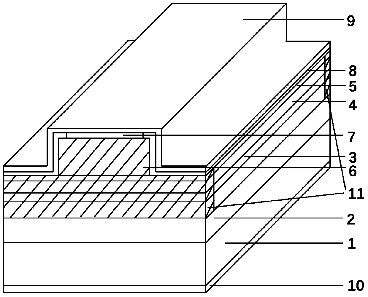
[0026] An AlGaInP semiconductor laser containing a highly selective corrosion barrier layer, comprising a substrate 1, a lower cladding layer 2, an active region 3, a first upper cladding layer 4, an corrosion barrier layer 5, and a second upper cladding layer from bottom to top. layer 6 and ohmic contact layer 7; the corrosion barrier layer 5 is arranged sequentially from bottom to top (Al a Ga 1-a ) 0.5 In 0.5 P, Ga b In 1-b P and (Al a Ga 1-a ) 0.5 In 0.5 P three-layer structure, the range of thickness of each layer is 5-15nm, wherein, the value of a is 0.1-0.5, and the value of b is 0.5-0.7; the active region 3 is arranged in sequence from bottom to top (Al x Ga 1-x ) 0.5 In 0.5 P barrier layer, Ga y In 1-y P quantum well and (Al x Ga 1-x ) 0.5 In 0.5 P barrier layer, wherein, the value of x is 0.4-0.6, and the value of y is 0.4-0.6; and the values of b and y satisfy the condition: b>y. The lasing wavelength of the active region is about 650nm.
Embodiment 2
[0028] A kind of AlGaInP semiconductor laser containing a highly selective etching barrier layer as described in Embodiment 1, the difference is that the second upper cladding layer 6 and the ohmic contact layer 7 form a ridge structure, and the second upper cladding layer 6 and the ohmic contact layer 7 form a ridge structure. The part of the layer 6 that does not cover the ohmic contact layer 7, the side surfaces of the second upper cladding layer 6 and the exposed corrosion barrier layer 5 are respectively coated with a dielectric film 8; above the ohmic contact layer 7, the coating contact is provided with a first The metal electrode layer 9 is provided with a second metal electrode layer 10 under the substrate 1; non-absorption windows 11 are provided at the front and rear end surfaces of the AlGaInP semiconductor laser.
Embodiment 3
[0030] A kind of AlGaInP semiconductor laser that contains highly selective etching barrier layer as described in embodiment 1, 2, its difference is that, described lower cladding layer, first upper cladding layer and second upper cladding layer are all with GaAs crystal lattice Matched Al 0.5 In 0.5 p.
PUM
 Abstract
Description
Claims
Application Information
 - R&D Engineer
- R&D Manager
- IP Professional
- Industry Leading Data Capabilities
- Powerful AI technology
- Patent DNA Extraction
Browse by: Latest US Patents, China's latest patents, Technical Efficacy Thesaurus, Application Domain, Technology Topic, Popular Technical Reports.
© 2024 PatSnap. All rights reserved.Legal|Privacy policy|Modern Slavery Act Transparency Statement|Sitemap|About US| Contact US: help@patsnap.com


