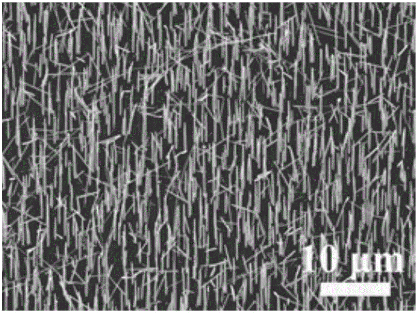
SiC nano array
A nano-array and nano-array technology, applied in nanotechnology, nanotechnology, nanotechnology for materials and surface science, etc., can solve the problems of restricting the growth direction of products, expensive carbon nanotubes, and self-consumption, etc., to achieve Ease of industrial production, effective distribution density and size, and low-cost effects
- Summary
- Abstract
- Description
- Claims
- Application Information
AI Technical Summary
Problems solved by technology
Method used
Image
Examples
Embodiment 1
[0042] In this embodiment, the SiC nano-array includes a substrate and a nano-array formed on the surface of the substrate,
[0043] The nanoarray is an arrangement of SiC nanowires, wherein the SiC crystal form in the SiC nanowires is C type, H type or R type; the SiC nanowires are needle-like structures with a thick bottom and a thin top (SiC nanowires can also be a linear structure)
[0044] The array density of nanowires in SiC nanoarrays is (5.0-6.0)×10 7 root / cm 2 (Preferably (5.2-5.7)×10 7 root / cm 2 ).
Embodiment 2
[0046] In this embodiment, the SiC nano-array includes a substrate and a nano-array formed on the surface of the substrate. The substrate is a SiC substrate, and the lattice structure of the SiC substrate includes 3C-SiC, 2H-SiC, 4H-SiC, 6H-SiC, 15R- Any of SiC;
[0047] The nanoarray is an arrangement of SiC nanowires, wherein the SiC crystal form in the SiC nanowires is C type, H type or R type; the SiC nanowires are needle-like structures with a thick bottom and a thin top (SiC nanowires can also be a linear structure)
[0048] The array density of nanowires in SiC nanoarrays is (5.0-6.0)×10 7 root / cm 2 .
Embodiment 3
[0050] In this embodiment, the SiC nano-array includes a substrate and a nano-array formed on the surface of the substrate. The substrate is a SiC substrate, and the lattice structure of the SiC substrate includes 3C-SiC, 2H-SiC, 4H-SiC, 6H-SiC, 15R- Any of SiC;
[0051] The nano-array is an arrangement of SiC nanowires, wherein the SiC crystal type in the SiC nanowires is C-type, H-type or R-type; the SiC nanowires have a needle-like structure with a thick bottom and a thin top (SiC nanowires can also be a linear structure), When SiC crystal form in SiC nanowire is C type, SiC is 3C-SiC; when SiC crystal form in SiC nanowire is H type, SiC is any of 2H-SiC, 4H-SiC, 6H-SiC; in SiC nanowire, SiC When the crystal form is R type, SiC is 15R-SiC;
[0052] The array density of nanowires in SiC nanoarrays is (5.0-6.0)×10 7 root / cm 2 .
PUM
| Property | Measurement | Unit |
|---|---|---|
| diameter | aaaaa | aaaaa |
| thickness | aaaaa | aaaaa |
| thickness | aaaaa | aaaaa |
Abstract
Description
Claims
Application Information
 - Generate Ideas
- Intellectual Property
- Life Sciences
- Materials
- Tech Scout
- Unparalleled Data Quality
- Higher Quality Content
- 60% Fewer Hallucinations
Browse by: Latest US Patents, China's latest patents, Technical Efficacy Thesaurus, Application Domain, Technology Topic, Popular Technical Reports.
© 2025 PatSnap. All rights reserved.Legal|Privacy policy|Modern Slavery Act Transparency Statement|Sitemap|About US| Contact US: help@patsnap.com


