
Organic light emitting diode package method and package structure and device containing structure

A technology of light-emitting diodes and encapsulation structures, which can be applied to organic semiconductor devices, electric solid-state devices, semiconductor devices, etc., and can solve problems such as OLED damage

Inactive Publication Date: 2015-11-25
BOE TECH GRP CO LTD
View PDF5 Cites 3 Cited by
  • Summary
  • Abstract
  • Description
  • Claims
  • Application Information

AI Technical Summary

Problems solved by technology

In addition, although the encapsulation glue is used to protect the OLED in this structure, water and oxygen will still penetrate into the OLED encapsulation structure through the encapsulation glue, thereby causing damage to the OLED.

Method used


Image

  • Organic light emitting diode package method and package structure and device containing structure
  • Organic light emitting diode package method and package structure and device containing structure
  • Organic light emitting diode package method and package structure and device containing structure

Examples


example 1

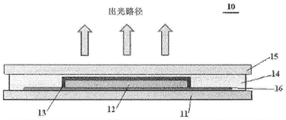
[0032] Set a 50 μm thick Invar alloy as the first substrate, form a 0.5 μm thick SiNx film on it as a flat layer by CVD, make an OLED on the flat layer, and use CVD to form a 1 μm thick SiNx film as a passivation layer , where the passivation layer covers the OLED. Coating encapsulation glue on the surface of the first substrate, covering the entire area of ​​the first substrate, at least setting a plastic film on the part of the encapsulation glue covering the passivation layer as the second substrate, the area of ​​the second substrate is smaller than the area of ​​the first substrate . The edge of the first substrate is folded so as to cover the second substrate and expose the light-emitting area, leaving one edge of the first substrate unfolded, thereby allowing the circuit part to extend to the outside. Finally, the encapsulation glue is cured to complete the encapsulation structure of the OLED.

example 2

[0034] Set a 100 μm thick Kovar alloy as the first substrate, heat and evenly paste a 0.5 μm thick plastic film on it as a flat layer, make an OLED structure on the flat layer, and use atomic force deposition (ALD) to form a 0.5 μm thick Al 2 o 3 The thin film acts as a passivation layer, where the passivation layer covers the OLED. Coating encapsulation glue on the surface of the first substrate, covering the entire area of ​​the first substrate, at least setting a plastic film on the part of the encapsulation glue covering the passivation layer as the second substrate, the area of ​​the second substrate is smaller than the area of ​​the first substrate . The edge of the first substrate is folded so as to cover the second substrate and expose the light-emitting area, and one edge of the first substrate is left unfolded, thereby allowing the circuit part to extend to the outside. Finally, the encapsulation glue is cured to complete the encapsulation structure of the OLED. ...


PUM


Abstract

The invention discloses a package method of an organic light emitting diode. The package method comprises the following steps of: arranging a first substrate, wherein the first substrate is made of metal foil; arranging the organic light emitting diode on the first substrate; arranging a passivation layer for covering the organic light emitting diode; coating package glue on the whole first substrate, wherein the package glue covers the passivation layer; arranging a second transparent substrate on at least part of the passivation layer covered with the package glue; and curving the package glue to form the package of the organic light emitting diode. The invention also discloses a package structure of the organic light emitting diode and an organic light emitting diode device containing the package structure.

Description

technical field [0001] The invention relates to the field of electronic components, in particular to an organic light emitting diode packaging method and packaging structure and an organic light emitting diode device with the packaging structure. Background technique [0002] Organic Light Emitting Diode (OLED) is a display lighting device that has gradually attracted attention in recent years, and it is especially favored by people because of its ability to realize flexible display. However, since the OLED device will be damaged due to corrosion under the action of water vapor and oxygen, the current OLED device needs the protection of the encapsulation structure. On the other hand, to realize the flexibility of OLEDs, it is required to use flexible substrates instead of traditional glass substrates. Currently used flexible substrates mainly include: ultra-thin glass, metal foil, plastic film, etc. Among them, because of the characteristics of easy handling and smooth sur...

Claims


Application Information

Patent Timeline
Patent Type & Authority Applications(China)
IPC IPC(8): H01L51/56H01L51/52
CPCH10K71/40H10K50/8426H10K50/846H10K50/844Y02E10/549H10K77/111H10K2102/3026H10K71/00H10K2102/00H10K2102/311
Inventor 罗程远王俊然
Owner BOE TECH GRP CO LTD
Learn More