GaN-based light-emitting diode (LED) epitaxy structure containing ternary superlattice and preparation method of GaN-based LED epitaxy structure

An epitaxial structure and superlattice technology, which is applied in the direction of electrical components, semiconductor/solid-state device manufacturing, circuits, etc., can solve the problems of reduced energy-saving service life, high resistance, etc., to reduce internal resistance, reduce dislocation defects, and improve load capacity. The effect of carrier concentration

Inactive Publication Date: 2015-11-25
GUANGXI SHENGHE ELECTRONICS TECH
View PDF3 Cites 5 Cited by
  • Summary
  • Abstract
  • Description
  • Claims
  • Application Information

AI Technical Summary

Problems solved by technology

[0004] Second, GaN is a crystal with high resistance. When the current flows through the LED, due to the large internal resistance, part of the electric energy will be converted into heat energy consumption, which greatly reduces the energy saving and service life of the LED.
[0007] Existing methods can improve crystal quality and reduce resistance to a certain extent, but there is still much room for improvement

Method used


Image

  • GaN-based light-emitting diode (LED) epitaxy structure containing ternary superlattice and preparation method of GaN-based LED epitaxy structure
  • GaN-based light-emitting diode (LED) epitaxy structure containing ternary superlattice and preparation method of GaN-based LED epitaxy structure
  • GaN-based light-emitting diode (LED) epitaxy structure containing ternary superlattice and preparation method of GaN-based LED epitaxy structure

Examples


Embodiment Construction

[0030] The following will clearly and completely describe the technical solutions in the embodiments of the present invention with reference to the accompanying drawings in the embodiments of the present invention. Obviously, the described embodiments are only some, not all, embodiments of the present invention. Based on the embodiments of the present invention, all other embodiments obtained by persons of ordinary skill in the art without creative efforts fall within the protection scope of the present invention.

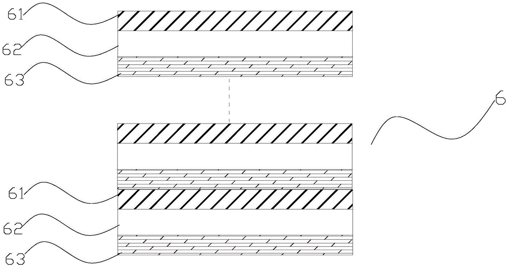
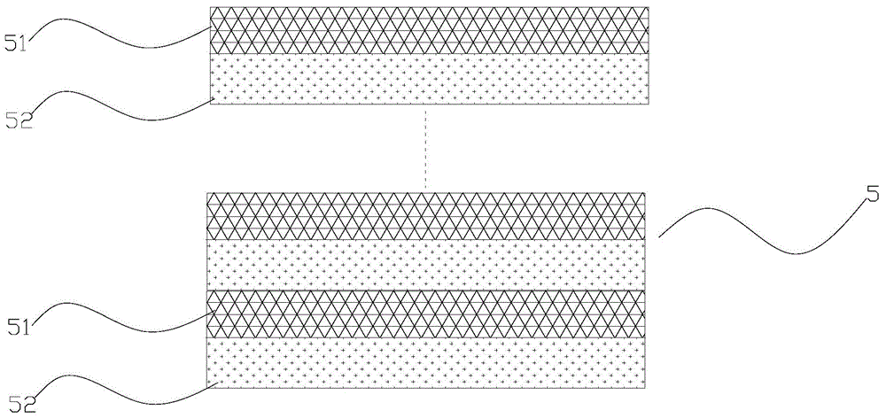
[0031] see figure 1 , figure 2 and image 3 As shown, the present invention provides a GaN-based LED epitaxial structure containing a ternary superlattice, including a sequentially stacked pattern substrate 1, buffer layer 2, non-doped intrinsic GaN layer 3, N-type GaN layer 4, multiple InGaN / GaN quantum well active layer 5, ternary superlattice layer 6 and P-type GaN layer 7, said ternary superlattice layer is grown by InGaN layer 61, AlGaN layer 62, A ternary...


PUM


Abstract

The invention relates to the technical field of luminescence of semiconductors, in particular to a GaN-based light-emitting diode (LED) epitaxy structure containing a ternary superlattice and a preparation method of the GaN-based LED epitaxy structure. According to the technical scheme, the GaN-based LED epitaxy structure comprises a patterned substrate, a buffer layer, a non-doped intrinsic GaN layer, an N-type GaN layer, a multi-InGaN / GaN quantum well active layer, a ternary superlattice layer and a P-type GaN layer, which are sequentially stacked; and the ternary superlattice layer is formed by growing the ternary superlattice which formed by an InGaN layer, an AlGaN layer and an MgGaN layer after growing a multi-quantum well layer. The GaN-based LED epitaxy structure has the beneficial effects that the dislocation defect of the quantum well layer and subsequent p-type GaN can be effectively reduced; the crystal quality of a GaN epitaxy film is improved; the carrier concentration can be effectively increased; and relatively good electronic blocking and diffusion are provided, so that the internal resistance is reduced, and the internal quantum efficiency is improved.

Description

technical field [0001] The invention relates to the technical field of semiconductor light emitting, in particular to a GaN-based LED epitaxial structure containing a ternary superlattice and a preparation method thereof. Background technique [0002] LED is a kind of solid light-emitting device that can directly convert electric energy into visible light and radiant energy. It has the advantages of long working life, high luminous efficiency, no pollution, light weight, small size, etc. It has developed by leaps and bounds and has been widely used in indoor and outdoor large Screen display, backlight display, lighting, decoration, traffic lights and other fields. The GaN material system is the most mature material for preparing blue, green, purple and ultraviolet LEDs. The research on GaN materials began in the 1930s. In 1991, someone in the industry discovered that the method of using a low-temperature growth GaN buffer layer can also greatly improve the quality of GaN ep...

Claims


Application Information

Patent Timeline
Patent Type & Authority Applications(China)
IPC IPC(8): H01L33/06H01L33/00H01L21/02
CPCH01L33/06H01L21/0242H01L21/02502H01L21/0254H01L21/0262H01L33/0066H01L33/0075
Inventor 段俊峰修川尹宝堂汤献忠
Owner GUANGXI SHENGHE ELECTRONICS TECH
Why Eureka
Try Eureka