A kind of polysilicon preparation device and method

A polysilicon preparation, amorphous silicon layer technology, applied in the growth of polycrystalline materials, chemical instruments and methods, crystal growth, etc. The effect of increasing electron mobility and increasing size

Active Publication Date: 2018-05-18
TCL CHINA STAR OPTOELECTRONICS TECH CO LTD
View PDF9 Cites 0 Cited by
  • Summary
  • Abstract
  • Description
  • Claims
  • Application Information

AI Technical Summary

Problems solved by technology

During recrystallization, it will crystallize from low energy to high energy, and from low temperature to high temperature; so the starting point and direction of crystallization are messy, such as figure 2 As shown; resulting in smaller grains after crystallization and more grain boundaries between grains, thus affecting the electron mobility of polysilicon

Method used


Image

  • A kind of polysilicon preparation device and method
  • A kind of polysilicon preparation device and method
  • A kind of polysilicon preparation device and method

Examples


Embodiment Construction

[0031] The word "embodiment" as used in this specification means serving as an example, instance or illustration. Furthermore, the article "a" as used in this specification and the appended claims may generally be construed to mean "one or more" unless specified otherwise or clear from context to refer to a singular form.

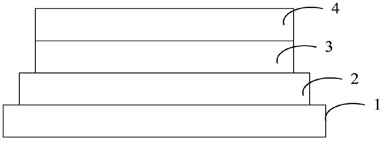
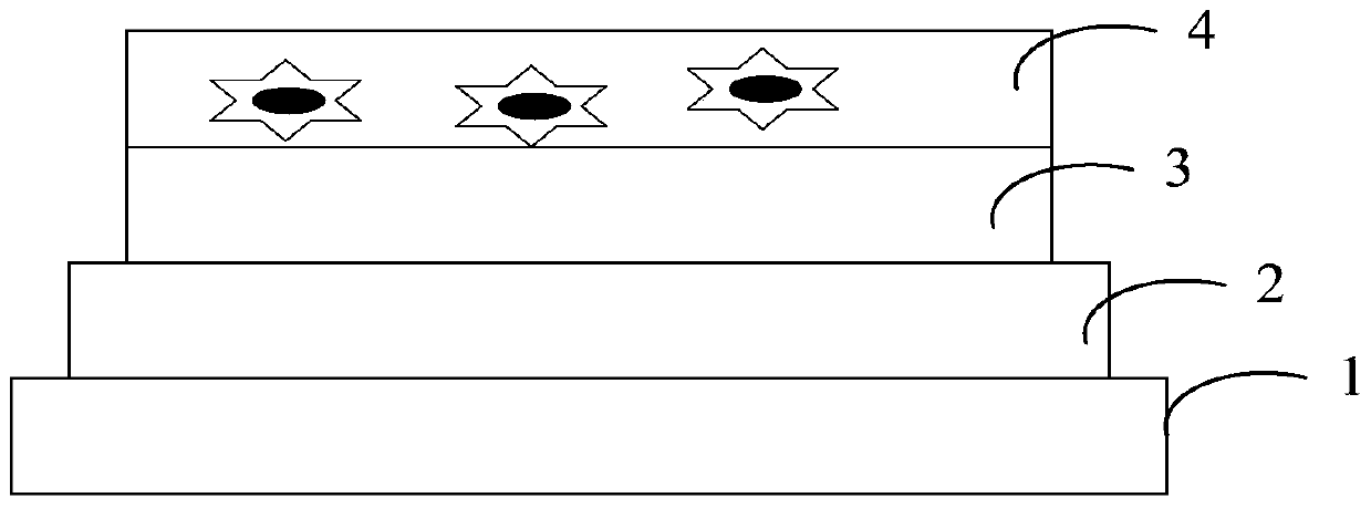
[0032] In the present invention, by arranging a plurality of reflection mirrors and a diffuse reflection layer on the surface of the support platform, the diffuse reflection layer is arranged between the reflection mirrors, and when laser annealing is performed, the diffuse reflection layer penetrates the When the laser light of the crystalline silicon layer is irradiated on the region of the diffuse reflection layer, diffuse reflection occurs; It absorbs energy and forms an energy gradient with other regions. Therefore, it is possible to control the crystallographic direction and the growth direction of polysilicon when it is formed, increase the size of ...


PUM


Abstract

The invention discloses a polysilicon preparation device comprising: a support platform, a reflective layer is arranged on the surface of the support platform, the reflective layer has a plurality of reflective mirrors and a diffuse reflective layer, and the diffuse reflective layer is arranged on the reflective Between the mirror and the reflecting mirror, a glass substrate is arranged on the reflective layer, a buffer layer is arranged on the glass substrate, and an amorphous silicon layer is arranged on the buffer layer; when performing laser annealing, the wear Diffuse reflection occurs when the laser light penetrating the amorphous silicon layer is irradiated on the diffuse reflection layer region; when it is irradiated on the mirror region, the reflected laser light can be focused on the amorphous silicon layer, so that the Amorphous silicon can absorb energy and form an energy gradient with other regions. The invention can control the crystallization direction and the growth direction when polysilicon is formed, increase the size of crystal grains, and increase the electron mobility of polysilicon.

Description

【Technical field】 [0001] The invention relates to the field of display technology, in particular to a polysilicon preparation device and method. 【Background technique】 [0002] With the development of flat-panel displays, the demand for high-resolution and low-power panels is constantly being raised. Amorphous silicon has low electron mobility, and low-temperature polysilicon can be produced at low temperatures, and has high electron mobility, and can be made into C- MOS circuits are therefore widely studied to meet the demands of high resolution and low power consumption of panels. [0003] The current methods for producing low-temperature polysilicon include: solid phase crystallization (SPC), metal-induced crystallization (MIC) and excimer laser annealing (ELA), among which excimer laser annealing is currently the most widely used method. [0004] Such as figure 1 As shown; the polysilicon preparation device includes: a support platform 1, a glass substrate 2 is arrange...

Claims


Application Information

Patent Timeline
Patent Type & Authority Patents(China)
IPC IPC(8): C30B28/02C30B29/06C30B30/00
Inventor 余威
Owner TCL CHINA STAR OPTOELECTRONICS TECH CO LTD
Why Eureka
Try Eureka