


Quick Research
Generate reliable direction feasibility study reports for your R&D in just a few steps.

Technical Q&A
Discover and master advanced knowledge NOW. Basics, ideas, possibilities, all at once.

Find Solutions
As an expert in R&D theories, this can generate solutions to your technical problems instantly.

Evaluate Feasibility
Analyze your overall solution with one click, know your potential R&D risks in advance.

Monitor Landscape
Get weekly tech updates, stay abreast of the latest tech innovations and key insights.
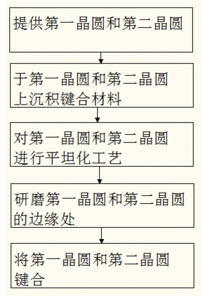
Wafer-level chip packaging method
A technology of wafer-level chips and packaging methods, which is applied in the manufacture of electrical components, electrical solid devices, semiconductor/solid devices, etc., and can solve problems such as surface mount process difficulties, chip chipping, and missing corners.
- Summary
- Abstract
- Description
- Claims
- Application Information
AI Technical Summary
Problems solved by technology
Method used
Image

Examples
Embodiment Construction
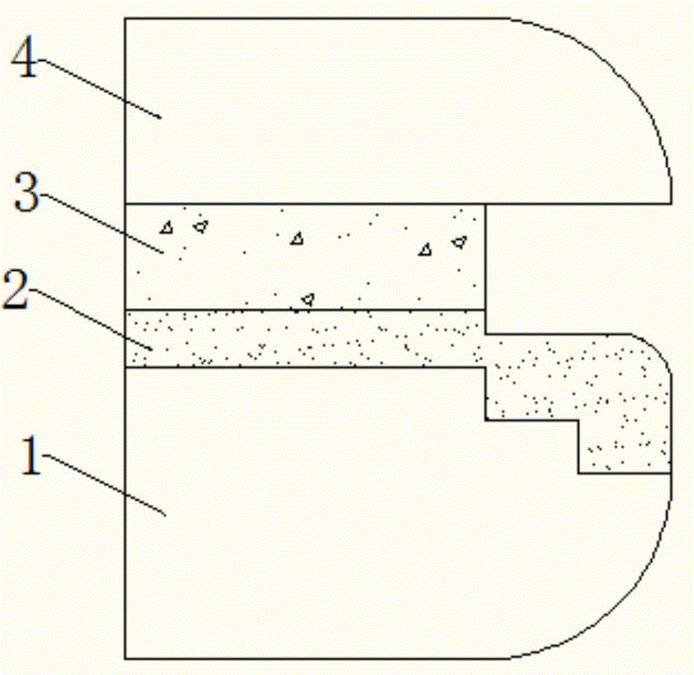
[0021] In order to make the technical solutions and advantages of the present invention more comprehensible, further details will be described below in conjunction with the accompanying drawings. It should be noted that the specific embodiments described here are only used to explain the present invention, not to limit the present invention.
[0022] The biggest feature of the wafer-level chip packaging method is that its package size is small, the inductance between the IC and the PCB is small, and the production cycle is shortened, so it can be used in portable products and meets the requirements of light, thin, and small. Information The transmission path is short, the stability is high, and the heat dissipation is good.
[0023] Since the wafer-level chip package lacks the traditional sealed plastic or ceramic package, the heat of the IC chip can be effectively dissipated during operation without increasing the temperature of the host. This feature has many benefits for th...
PUM
 Abstract
Description
Claims
Application Information
 - R&D Engineer
- R&D Manager
- IP Professional
- Industry Leading Data Capabilities
- Powerful AI technology
- Patent DNA Extraction
Browse by: Latest US Patents, China's latest patents, Technical Efficacy Thesaurus, Application Domain, Technology Topic, Popular Technical Reports.
© 2024 PatSnap. All rights reserved.Legal|Privacy policy|Modern Slavery Act Transparency Statement|Sitemap|About US| Contact US: help@patsnap.com