Near infrared detector based on resonance tunneling effect
A resonant tunneling and detector technology, used in semiconductor devices, semiconductor/solid-state device manufacturing, electrical components, etc. The effect of reducing shot noise
- Summary
- Abstract
- Description
- Claims
- Application Information
AI Technical Summary
Problems solved by technology
Method used
Image
Examples
Embodiment Construction
[0020] It should be noted that implementations not shown or described in the accompanying drawings are forms known to those of ordinary skill in the art. Additionally, while illustrations of parameters including particular values may be provided herein, it should be understood that the parameters need not be exactly equal to the corresponding values, but rather may approximate the corresponding values within acceptable error margins or design constraints. In addition, the directional terms mentioned in the following embodiments only refer to the directions of the drawings. Accordingly, the directional terms are used to illustrate and not to limit the invention.
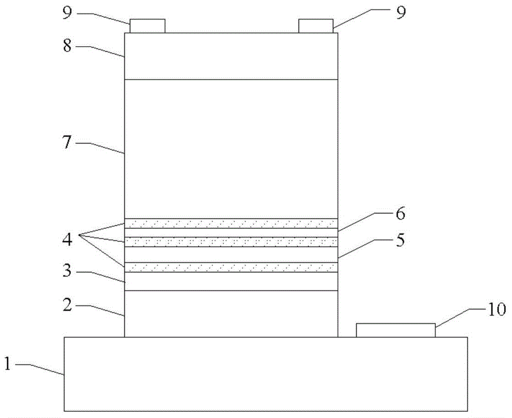
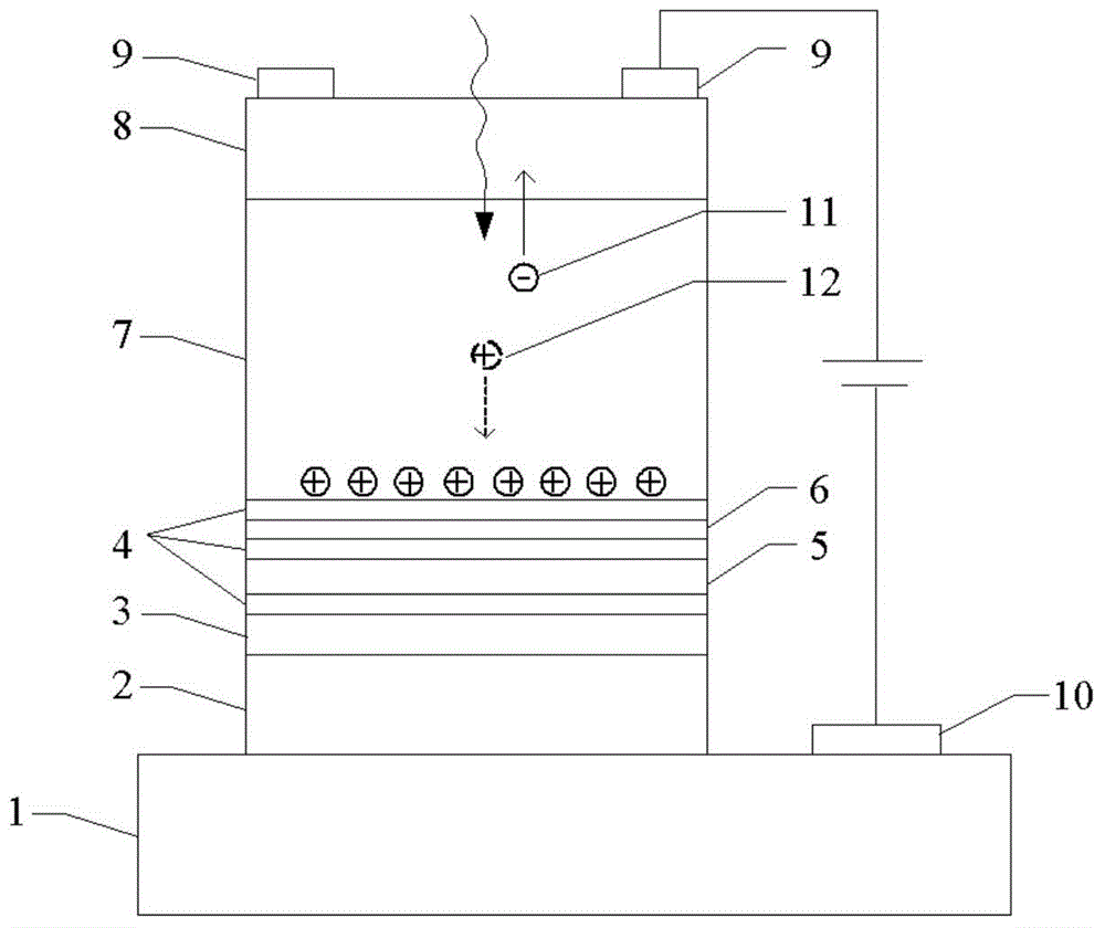
[0021] In an exemplary embodiment of the present invention, a molecular beam epitaxy technique is provided, according to figure 1 The structure shown, the method for preparing a high-sensitivity near-infrared detector.
[0022] First, the epitaxial growth thickness is 100nm and the doping concentration is 2×10 o...
PUM
 Abstract
Description
Claims
Application Information
 - R&D
- Intellectual Property
- Life Sciences
- Materials
- Tech Scout
- Unparalleled Data Quality
- Higher Quality Content
- 60% Fewer Hallucinations
Browse by: Latest US Patents, China's latest patents, Technical Efficacy Thesaurus, Application Domain, Technology Topic, Popular Technical Reports.
© 2025 PatSnap. All rights reserved.Legal|Privacy policy|Modern Slavery Act Transparency Statement|Sitemap|About US| Contact US: help@patsnap.com


