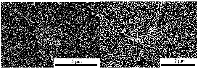
Method and application of low-temperature in-situ growth of nanostructured semiconductor metal oxides
A nanostructure and in-situ growth technology, applied in the field of nanomaterials, can solve the problems that flexible organic and polymer material substrates cannot withstand high temperatures, limit the use of flexible polymer substrates, and make it difficult to develop and apply flexible optoelectronic devices. Effects of charge transfer, enhanced binding, and step-by-step convenience
- Summary
- Abstract
- Description
- Claims
- Application Information
AI Technical Summary
Problems solved by technology
Method used
Image
Examples
Embodiment 1
[0034] The preparation method of the method of the present invention comprises the following steps:
[0035]1. prepare the mixed solution of stannous chloride and polyvinyl butyral, i.e. spinning solution, the concentration of said stannous chloride is 85 mg / mL, and the concentration of polyvinyl butyral is 40 mg / mL; wherein Stannous chloride can be any metal salt that can be dissolved in the spinning solution solvent and has good compatibility with spinning aids, including but not limited to stannous chloride, tin tetrachloride, tetrabutyl titanate , tetraisopropyl titanium, zinc chloride, zinc acetate, ferric chloride, ferric nitrate; polyvinyl butyral can be any one or more oil-soluble polymers, including but not limited to polyvinyl butyral Aldehyde, polyvinylidene fluoride, polyvinyl chloride;
[0036] ② Deposit the electrospinning solution in step ① in the form of nanofibers on the ceramic substrate under the electrospinning conditions of flow rate 0.2mL / h; receiving di...
Embodiment 2
[0041] 1. prepare the mixed solution of zinc acetate and polyvinyl butyral, i.e. spinning solution, the concentration of zinc acetate is 10mg / mL, and the concentration of polyvinyl butyral is 100 mg / mL;
[0042] ②The electrospinning solution in step ① was deposited on the polyterephthalene in the form of nanofibers under the electrospinning conditions of flow rate 0.1mL / h; receiving distance 5cm; spinning voltage 5kV; receiving time 30 min. on a glycol formate substrate;
[0043] ③ drying the substrate deposited with nanofibers obtained in step ② and then hydrothermally treating it at 180° C. for 24 h to obtain a substrate with a semiconductor metal oxide nanostructure grown in situ, and the preparation method;
[0044] ④ In-situ polymerization and growth of polypyrrole on the substrate with the semiconductor metal oxide nanostructure obtained in step ③ to prepare a gas sensor.
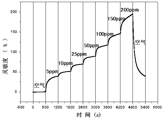
[0045] The resulting method exhibited a low resistance of less than 170 kΩ at low concentrations ...
Embodiment 3
[0047] 1. prepare the mixed solution of tin chloride and polyvinyl chloride, i.e. spinning solution, the concentration of said tin chloride is 300 mg / mL, and the concentration of polyvinyl chloride is 40 mg / mL;
[0048] ② The electrospinning solution in step ① was deposited in the form of nanofibers on the polystyrene under the electrospinning conditions of flow rate of 1 mL / h; receiving distance of 30 cm; spinning voltage of 30 kV; receiving time of 0.5 min. on vinyl fluoride substrates;
[0049] ③ drying the substrate deposited with nanofibers obtained in step ② and then hydrothermally treating it at 120° C. for 6 h to obtain a substrate with a semiconductor metal oxide nanostructure grown in situ, and the preparation method;
[0050] ④ In-situ polymerization and growth of polypyrrole on the substrate with the semiconductor metal oxide nanostructure obtained in step ③ to prepare a gas sensor.
[0051] The resulting method has a low impedance of less than 200 kΩ at low conce...
PUM
| Property | Measurement | Unit |
|---|---|---|
| concentration | aaaaa | aaaaa |
Abstract
Description
Claims
Application Information
 - R&D
- Intellectual Property
- Life Sciences
- Materials
- Tech Scout
- Unparalleled Data Quality
- Higher Quality Content
- 60% Fewer Hallucinations
Browse by: Latest US Patents, China's latest patents, Technical Efficacy Thesaurus, Application Domain, Technology Topic, Popular Technical Reports.
© 2025 PatSnap. All rights reserved.Legal|Privacy policy|Modern Slavery Act Transparency Statement|Sitemap|About US| Contact US: help@patsnap.com


