


Quick Research
Generate reliable direction feasibility study reports for your R&D in just a few steps.

Technical Q&A
Discover and master advanced knowledge NOW. Basics, ideas, possibilities, all at once.

Find Solutions
As an expert in R&D theories, this can generate solutions to your technical problems instantly.

Evaluate Feasibility
Analyze your overall solution with one click, know your potential R&D risks in advance.

Monitor Landscape
Get weekly tech updates, stay abreast of the latest tech innovations and key insights.
Elastic wave device
An elastic wave device, elastic wave resonator technology, applied in impedance network, transformer, electrical components and other directions, can solve the problems of inductance deviation, reduction of the 9Q value of the inductor electrode, etc.
- Summary
- Abstract
- Description
- Claims
- Application Information
AI Technical Summary
Problems solved by technology
Method used
Image

Examples
Embodiment approach 1
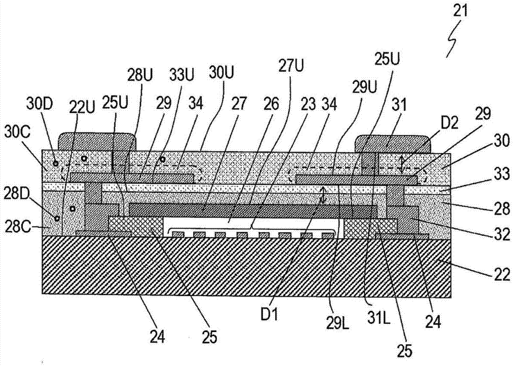
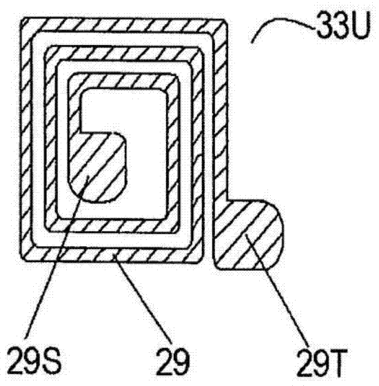
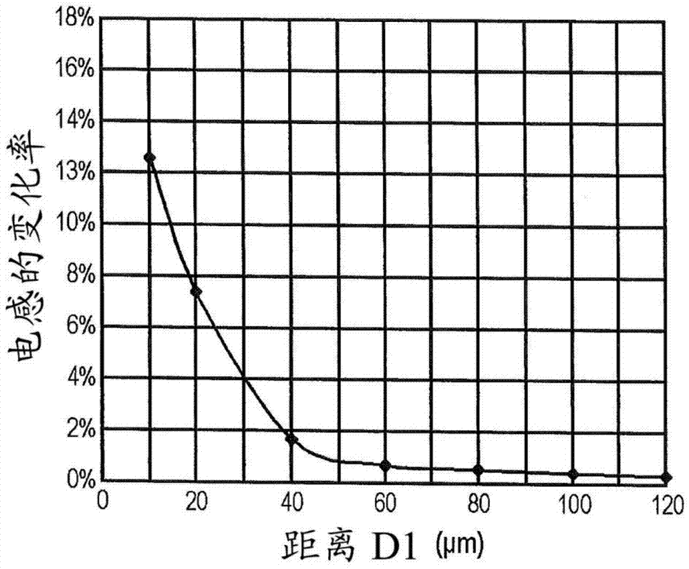
[0029] Figure 1A is a schematic cross-sectional view of elastic wave device 21 in Embodiment 1 of the present invention. The elastic wave device 21 includes: a piezoelectric substrate 22; an interdigital transducer (IDT) electrode 23 arranged on the upper surface 22U of the piezoelectric substrate 22; a wiring electrode 24 arranged on the upper surface 22U of the piezoelectric substrate 22; The side wall 25 arranged on the upper surface 22U of the piezoelectric substrate 22; the top electrode 27 arranged on the upper surface 25U of the side wall 25; the insulator 28 covering the side wall 25 and the top electrode 27; arranged on the upper surface of the insulator 28 The resin layer 33 on 28U; the inductor electrode 29 provided on the upper surface 33U of the resin layer 33; the insulator 30 covering the upper surface 33U of the resin layer 33 and the inductor electrode 29; terminal electrode 31 ; and connection electrode 32 penetrating through insulators 28 , 30 and resin la...
Embodiment approach 2
[0056] Figure 3A It is a schematic cross-sectional view of elastic wave device 111 in Embodiment 2 of the present invention. The elastic wave device 111 includes: a piezoelectric substrate 112; a plurality of interdigital transducer (IDT) electrodes 113 arranged on an upper surface 112U of the piezoelectric substrate 112; and wiring electrodes arranged on the upper surface 112U of the piezoelectric substrate 112. 114; the side wall 115 disposed on the upper surface 112U of the piezoelectric substrate 112; the adhesive layer 117 disposed on the upper surface 115U of the side wall 115; the top plate electrode 118 disposed on the upper surface 117U of the adhesive layer 117; The insulator 119 provided on the upper surface 112U of the piezoelectric substrate 112; the inductor electrode 120 arranged on the upper surface 119U of the insulator 119; the insulator 121 arranged on the upper surface 119U of the insulator 119; the upper surface of the insulator 121 arranged terminal ele...
Embodiment approach 3
[0089] Figure 4 It is a circuit diagram of elastic wave device 191 in Embodiment 3 of the present invention. Figure 5 is a schematic cross-sectional view of the elastic wave device 191 . exist Figure 4 and Figure 5 In the drawings in Embodiment 3, for and Figure 3A The same components of the elastic wave device 111 in the second embodiment shown are given the same reference numerals.
[0090] like Figure 4 As shown, the elastic wave device 191 is a duplexer including a transmission filter 129 and a reception filter 130 . The input and output terminals of the transmission filter 129 are an unbalanced transmission-side signal terminal 135A, a transmission-side ground terminal 135B, and an antenna terminal 135C. The input and output terminals of the reception filter 130 are a balanced reception-side signal terminal 135D, a reception-side ground terminal 135E, and an antenna terminal 135C. In the reception filter 130, two longitudinally coupled resonator-type elastic ...
PUM
 Abstract
Description
Claims
Application Information
 - R&D Engineer
- R&D Manager
- IP Professional
- Industry Leading Data Capabilities
- Powerful AI technology
- Patent DNA Extraction
Browse by: Latest US Patents, China's latest patents, Technical Efficacy Thesaurus, Application Domain, Technology Topic, Popular Technical Reports.
© 2024 PatSnap. All rights reserved.Legal|Privacy policy|Modern Slavery Act Transparency Statement|Sitemap|About US| Contact US: help@patsnap.com