Covering type super-junction transverse double diffusion metal oxide semiconductor field effect transistor with N-type buried layer

An oxide semiconductor, lateral double diffusion technology, applied in semiconductor devices, electrical components, circuits, etc., can solve problems such as breaking the charge balance, reducing the lateral breakdown voltage of SJ-LDMOS devices, and the inability of the P-type column region to be completely depleted. , to achieve high breakdown voltage, low specific on-resistance, and improve the effect of contradictory relationship

Active Publication Date: 2015-06-24
XIDIAN UNIV
View PDF3 Cites 0 Cited by
  • Summary
  • Abstract
  • Description
  • Claims
  • Application Information

AI Technical Summary

Problems solved by technology

[0004] However, for SJ-LDMOS, due to the substrate-assisted depletion of the N-type pillar region (or P-type pillar region), the P-type pillar region (or N-type pillar region) cannot be completely depleted when the device breaks down, breaking the N-type pillar region. The charge balance between the column area and the P-type column area reduces the lateral breakdown voltage of the SJ-LDMOS device

Method used


Image

  • Covering type super-junction transverse double diffusion metal oxide semiconductor field effect transistor with N-type buried layer
  • Covering type super-junction transverse double diffusion metal oxide semiconductor field effect transistor with N-type buried layer

Examples


Embodiment Construction

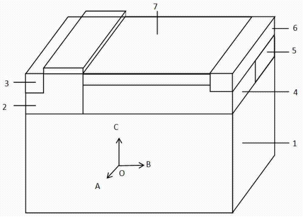
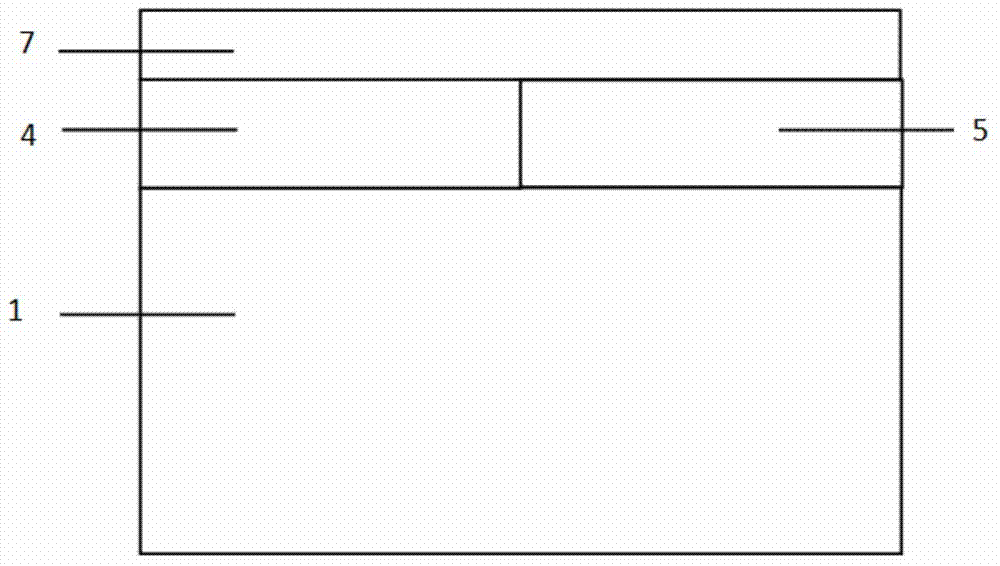
[0025] see figure 1 and figure 2 In the following, an N-type buried-layer-covered (N-channel) superjunction lateral double-diffused metal-oxide-semiconductor field effect transistor is taken as an example to specifically introduce the new structure in the embodiment of the present invention. Those skilled in the art should be able to recognize that this embodiment does not limit the protection scope of the present invention.

[0026] The N-type buried layer covered semi-superjunction lateral double-diffused metal oxide semiconductor field effect transistor includes:

[0027] P-type semiconductor substrate 1;

[0028] The P-type base region 2 and the super junction region adjacent to the surface of the N-type epitaxial layer on the P-type semiconductor substrate 1; the super junction region adopts the N-type column region 4 and the P-type column region 5 to be arranged at intervals in a lateral period ( A period is simplified in the figure), the width of each N-type column ...


PUM


Abstract

The invention discloses a new SJ-LDMOS device, and belongs to the technical field of semiconductor power devices. An N-type buried layer is introduced in a traditional SJ-LDMOS device structure and located on a super-junction layer. Compared with a traditional SJ-LDMOS, by means of the action of the N-type buried layer, charge imbalance between an N-type column region and a P-type column region in a super junction is compensated, the substrate-assisted effect is overcome, and breakdown voltage is increased; due to the N-type buried layer, a new conduction path is additionally added, and specific on-resistance is reduced. The structure has the advantages of the high breakdown voltage, the low on-resistance and charge balance in the super-junction layer. The new SJ-LDMOS device structure has the advantages of being simple in manufacturing technology and low in technology difficulty and meets the application requirement of a power electronic system more easily.

Description

technical field [0001] The invention relates to the technical field of semiconductor power devices, in particular to a superjunction lateral double-diffused metal oxide semiconductor field effect transistor. Background technique [0002] Lateral Double-diffused MOSFET (LDMOS for short) has become a key device in the design of intelligent power integrated circuits and system-on-chip due to its advantages such as easy integration with low-voltage devices. Its main feature is that a relatively long lightly doped drift region is added between the base region and the drain region. The doping type of the drift region is consistent with that of the drain region. By adding the drift region, it can share the breakdown voltage. Improve the breakdown voltage of LDMOS. The optimization goal of LDMOS is low on-resistance, which minimizes conduction losses. [0003] The super junction (super junction) structure is alternately arranged N-type pillar regions and P-type pillar regions. If ...

Claims


Application Information

Patent Timeline
Patent Type & Authority Applications(China)
IPC IPC(8): H01L29/78H01L29/06
Inventor 段宝兴马剑冲杨银堂李春来袁嵩
Owner XIDIAN UNIV
Why Eureka
Try Eureka