Detection method of storage unit in sram

A detection method and storage unit technology, applied in static memory, instruments, etc., can solve the problems of time-consuming, inaccurate, and high cost of storage units, and achieve the effects of accurate results, reduced detection amount, and low cost

Active Publication Date: 2017-09-22
SEMICON MFG INT (SHANGHAI) CORP
View PDF6 Cites 0 Cited by
  • Summary
  • Abstract
  • Description
  • Claims
  • Application Information

AI Technical Summary

Problems solved by technology

[0010] The present invention solves the problem of high cost, time-consuming and inaccurate detection of memory cells in SRAM through wafer acceptability test

Method used


Image

  • Detection method of storage unit in sram
  • Detection method of storage unit in sram
  • Detection method of storage unit in sram

Examples


Embodiment Construction

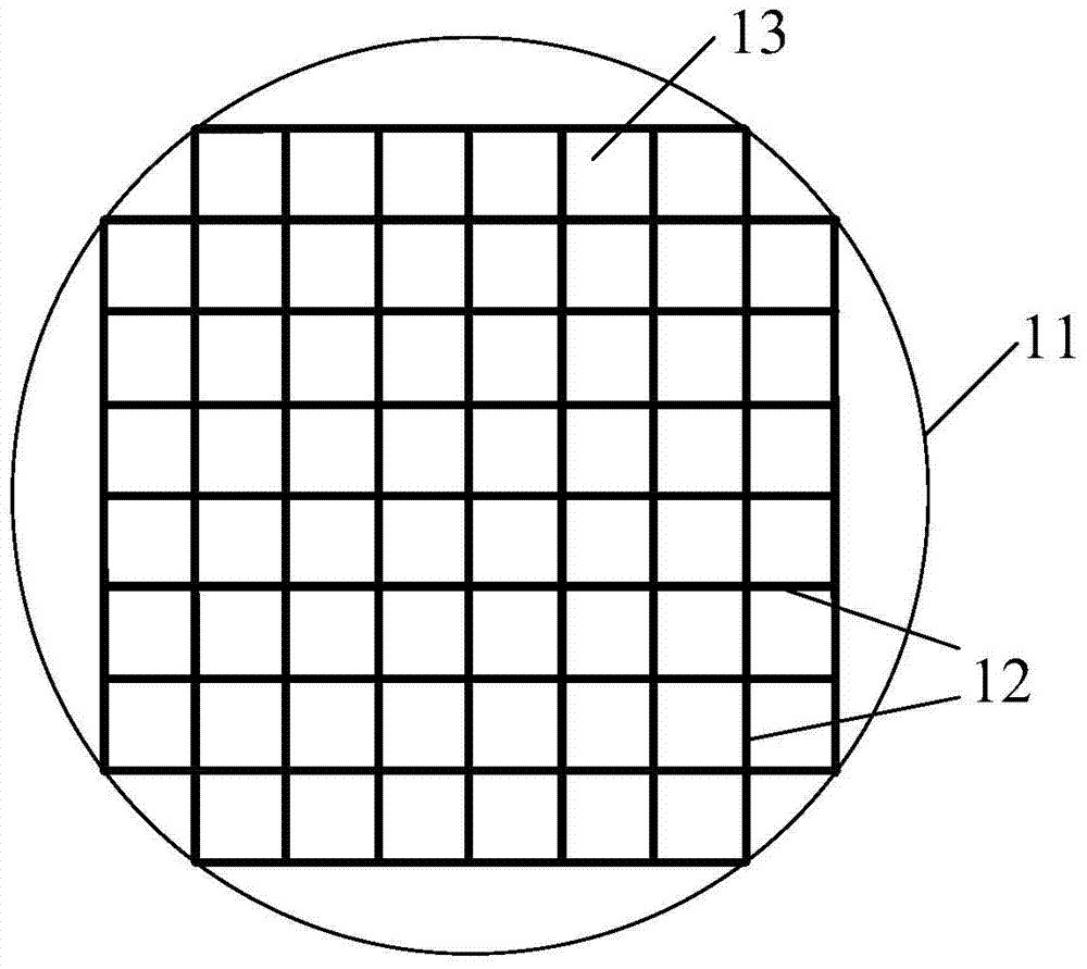
[0048] As described in the background technology, the existing method for detecting SRAM memory cells is to scan each MOS transistor in the memory cell to obtain the threshold voltage of each MOS transistor, and SRAM has a plurality of memory cells, which results in obtaining the memory cell Whether the two inverters are matched is costly and time-consuming, and sometimes the result is not accurate. In view of the above problems, the present invention proposes to perform detection in units of storage units, which reduces the amount of testing, improves efficiency, and provides more accurate results.

[0049] In order to make the above objects, features and advantages of the present invention more comprehensible, specific embodiments of the present invention will be described in detail below in conjunction with the accompanying drawings.

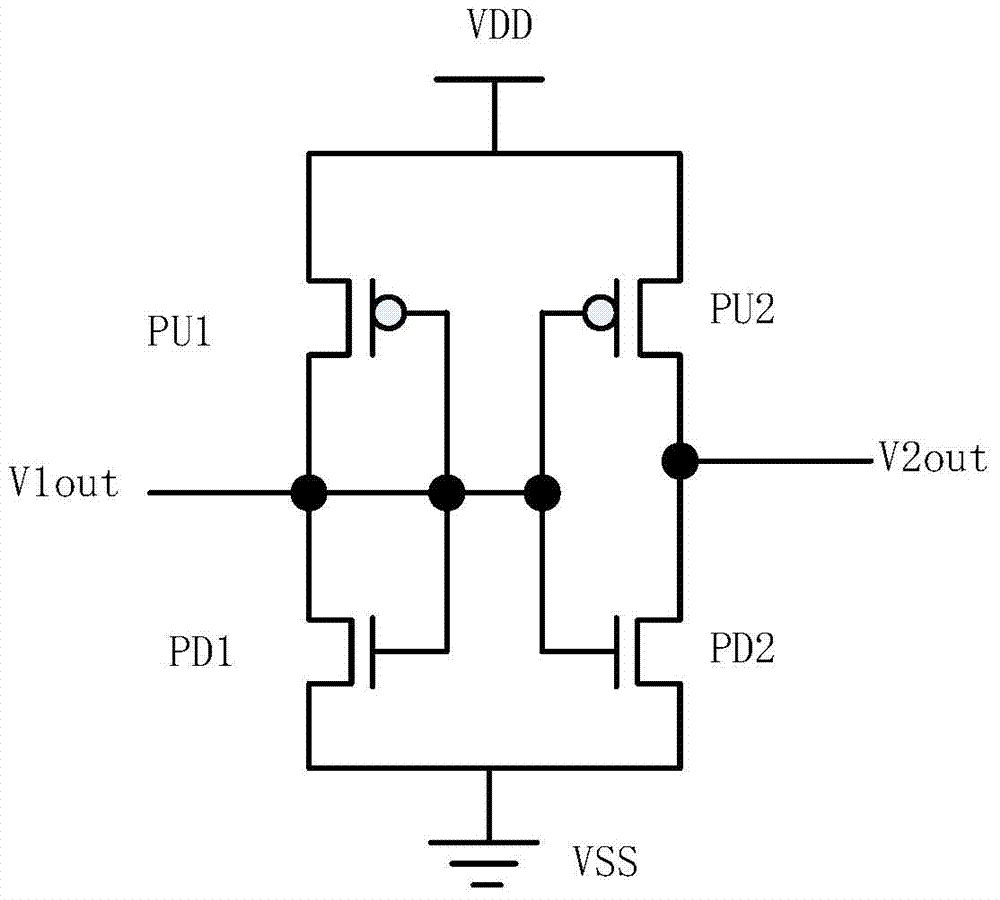
[0050] image 3 It is a circuit diagram used in the detection method provided by an embodiment of the present invention, refer to image 3...


PUM


Abstract

A method for detecting a storage unit in an SRAM, by connecting the input terminal of the first inverter in the storage unit to the output terminal and the input terminal of the second inverter, using the first inverter The input and output of the second inverter are equal, and the input and output of the second inverter conform to the characteristic curve of the inverter. If the two inverters match, when the input of the first inverter is equal to the input of the second inverter , the output of the first inverter must be equal to the output of the second inverter; and then it can be concluded that in the case that the input of the first inverter is equal to the input of the second inverter, the first inverter If the output of the second inverter is not equal to that of the second inverter, the two inverters do not match, and there must be at least one transistor whose threshold voltage drifts. Using the storage unit as the detection unit avoids separate detection of each MOS transistor in the storage unit, reduces the detection amount of the entire SRAM, improves efficiency, and has low cost and accurate results.

Description

technical field [0001] The invention relates to the technical field of integrated circuits, in particular to a method for detecting a storage unit in an SRAM. Background technique [0002] With the improvement of integrated circuit integration and the reduction of power supply voltage, the geometric size of semiconductor devices constituting integrated circuits has been continuously reduced, which requires continuous improvement of chip manufacturing processes. The improvement of the manufacturing process has a great influence on the performance of a single semiconductor device. In order to evaluate the performance of the semiconductor device, it is usually necessary to test the reliability of the semiconductor device. [0003] There are a large number of memory cells composed of two inverters in SRAM (Static Random Access Memory). Each inverter includes a pair of pull-up PMOS transistors and pull-down NMOS transistors. If the two inverters do not match, the The data of the...

Claims


Application Information

Patent Timeline
Patent Type & Authority Patents(China)
IPC IPC(8): G11C29/50
Inventor 王楠李煜王媛王颖倩
Owner SEMICON MFG INT (SHANGHAI) CORP
Why Eureka
Try Eureka