Optical memristor based on metamaterials
A memristor and sheet-like technology, which is applied in the field of waveguide memristors, can solve the problems of memristors that have not been reported before, and achieve the effect of rich functions, low cost, and easy insertion and removal
- Summary
- Abstract
- Description
- Claims
- Application Information
AI Technical Summary
Problems solved by technology
Method used
Image

Examples
Embodiment 1
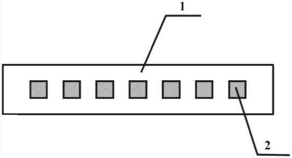
[0030] The structure of the optical memristor obtained in this embodiment is as follows figure 1 As shown, it consists of 7 photomemristors 2 and filling medium 1;
[0031] Among them, seven memristors 2 are located in the filling medium 1;
[0032] The material constituting the photomemristor is calcium titanate particles with a particle size of 1 μm-2 μm, a dielectric constant of 110, and a dielectric loss tangent of 0.002;
[0033] The material constituting the filling medium is polytetrafluoroethylene, a material transparent to the frequency band used by the optical memristor;
[0034] Each photomemristor can be prepared as follows: Calcium titanate particles with a particle size of 1 μm-2 μm, a dielectric constant of 110, and a dielectric loss tangent of 0.002 are sintered at 1400 ° C, cooled to room temperature, and cut into lengths and widths A cube with a height of 2mm is obtained.
Embodiment 2
[0036] The optical memristor sheet obtained in this embodiment is composed of an optical memristor and a filling medium;
[0037] Wherein, the optical memristor is located in the filling medium.
[0038] The photomemristor is a copper ring body with a notch on the copper ring; the side length of the copper ring is 4mm, the width is 0.5mm, and the notch is 0.3mm. The gap part is equivalent to the capacitance C, and the other metal parts are equivalent to the inductance L;
[0039] The material constituting the filling medium is polytetrafluoroethylene which is transparent to the operating frequency band of the optical memristor.
Embodiment 3
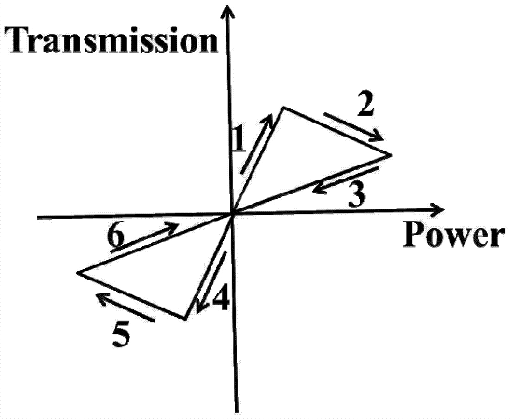
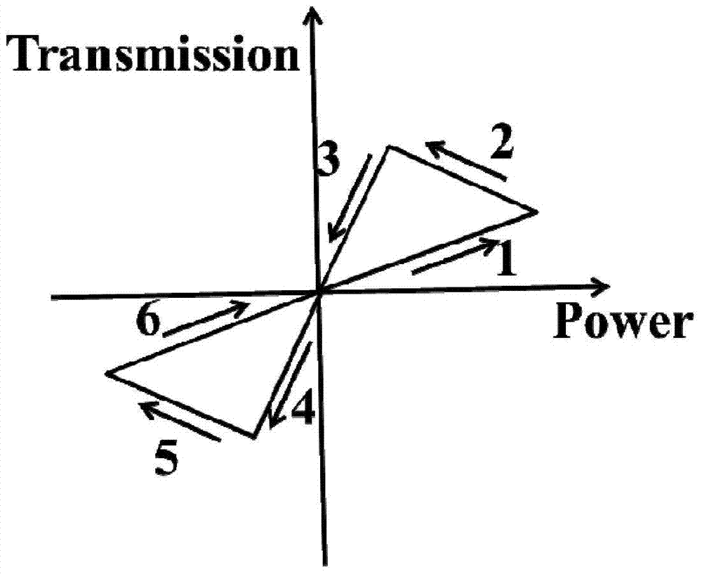
[0041] The performance of the optical memristor sheet obtained in Examples 1 and 2 can be checked using a vector network analyzer,
[0042] The vector network analyzer has the functions of power sweep, time sweep and linear frequency sweep, and can well detect the performance of the prepared photomemristor.
[0043] Wherein, the photomemristive sheets obtained in Examples 1 and 2 all have the shape of figure 2 , image 3 , Figure 4 and Figure 5 the response to.
[0044] figure 2 The initial state of Zhongguang Memristor is a state of high transmittance. During the process of increasing the incident power, it undergoes a transition from high transmittance to low transmittance, and maintains this state of transmittance until a certain reverse power is applied. Reset from low transmittance to high transmittance. That is to say, as the incident field power increases, the transmittance of the photomemristor changes from high transmittance to low transmittance, and the sta...
PUM
 Abstract
Description
Claims
Application Information
 - R&D
- Intellectual Property
- Life Sciences
- Materials
- Tech Scout
- Unparalleled Data Quality
- Higher Quality Content
- 60% Fewer Hallucinations
Browse by: Latest US Patents, China's latest patents, Technical Efficacy Thesaurus, Application Domain, Technology Topic, Popular Technical Reports.
© 2025 PatSnap. All rights reserved.Legal|Privacy policy|Modern Slavery Act Transparency Statement|Sitemap|About US| Contact US: help@patsnap.com