A bimodal distribution nano-silver paste used as thermal interface material and preparation method thereof
A thermal interface material, bimodal distribution technology, used in semiconductor/solid-state device manufacturing, circuits, electrical solid-state devices, etc., can solve problems such as device failure, and achieve uniform size, high thermal conductivity, and stable and reliable process conditions.
- Summary
- Abstract
- Description
- Claims
- Application Information
AI Technical Summary
Problems solved by technology
Method used
Image
Examples
Embodiment 1
[0036] Example 1 Preparation of a bimodal distribution nano-silver paste used as a thermal interface material
[0037] Mix small-size nano-silver particles (average particle size 9nm), large-size nano-silver particles (average particle size 52nm) and ultrapure water at a mass ratio of 7:3:50, mechanically stir for 50 minutes, and ultrasonically disperse in ice water 40min, and then centrifuged at a speed of 4000rpm for 15min again to remove the upper layer solution to obtain the bimodal distribution nano-silver paste precipitated at the bottom.
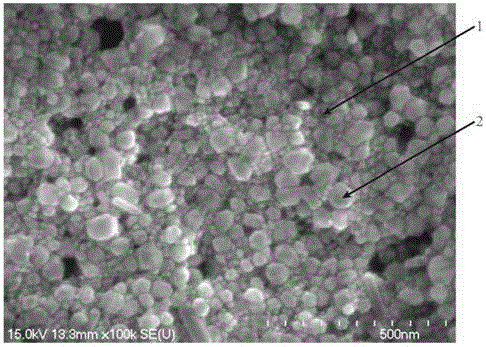
[0038] The SEM picture of the bimodal distribution nano-silver paste prepared by mixing is as follows figure 1 shown.
[0039] Apply bimodal distribution nano-silver paste on the surface of the interconnection between SiC chip and Cu substrate to form a sandwich structure of SiC chip / bimodal distribution nano-silver paste / Cu substrate, and place it on a heating plate at a temperature of 200°C for 20 minutes to form a sintered joint ...
Embodiment 2
[0040] Example 2 Preparation of a bimodal distribution nano-silver paste used as a thermal interface material
[0041] Mix small-size nano-silver particles (average particle size 21nm), large-size nano-silver particles (average particle size 117nm) and ultrapure water at a mass ratio of 2:1:12, mechanically stir for 30 minutes, and ultrasonically disperse in ice water 40min, and then centrifuged at a speed of 3000rpm for 10min again to remove the upper layer solution to obtain the bimodal distribution nano-silver paste precipitated at the bottom.
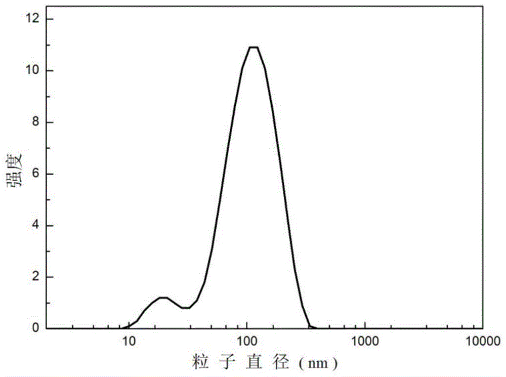
[0042] The laser particle size analyzer scanning image of the prepared uniformly mixed bimodal distribution nano-silver paste is as follows: figure 2 shown.
[0043] Apply bimodal distribution nano-silver paste on the surface of the interconnection between SiC chip and Cu substrate to form a sandwich structure of SiC chip / bimodal distribution nano-silver paste / Cu substrate, and place it on a heating plate at a temperature of 150°C...
Embodiment 3
[0044] Example 3 Preparation of a bimodal distribution nano-silver paste used as a thermal interface material
[0045] Mix small-size nano-silver particles (average particle size 15nm), large-size nano-silver particles (average particle size 81nm) and ultrapure water at a mass ratio of 3:2:30, mechanically stir for 30 minutes, and ultrasonically disperse in ice water 30min, and then centrifuged at a speed of 3000rpm for 20min again to remove the upper layer solution to obtain the bimodal distribution nano-silver paste precipitated at the bottom.
[0046] Apply bimodal distribution nano-silver paste on the surface of the interconnection between SiC chip and Cu substrate to form a sandwich structure of SiC chip / bimodal distribution nano-silver paste / Cu substrate, and place it on a heating plate at a temperature of 200°C for 30 minutes to form a sintered joint .
PUM
| Property | Measurement | Unit |
|---|---|---|
| particle diameter | aaaaa | aaaaa |
| particle diameter | aaaaa | aaaaa |
| thickness | aaaaa | aaaaa |
Abstract
Description
Claims
Application Information
 - R&D
- Intellectual Property
- Life Sciences
- Materials
- Tech Scout
- Unparalleled Data Quality
- Higher Quality Content
- 60% Fewer Hallucinations
Browse by: Latest US Patents, China's latest patents, Technical Efficacy Thesaurus, Application Domain, Technology Topic, Popular Technical Reports.
© 2025 PatSnap. All rights reserved.Legal|Privacy policy|Modern Slavery Act Transparency Statement|Sitemap|About US| Contact US: help@patsnap.com


