Anisotropic conductive film and semiconductor device using same
An anisotropic, conductive film technology, applied in the direction of semiconductor devices, semiconductor/solid-state device manufacturing, electric solid-state devices, etc., can solve problems such as reduced adhesion, fracture of anisotropic conductive film, and reduced film pre-compression properties. Effects of ensuring bonding force, improving connection reliability, and ensuring shape stability
- Summary
- Abstract
- Description
- Claims
- Application Information
AI Technical Summary
Problems solved by technology
Method used
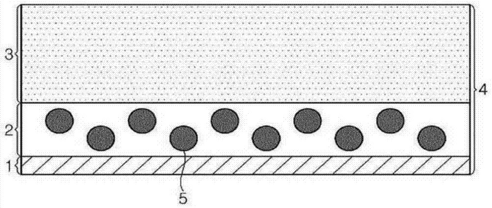
Image


Examples
preparation example Construction
[0149] The method of preparing an anisotropic conductive film according to an embodiment of the present invention is not particularly limited, and any specific method known in the art may be used without limitation.
[0150] No special equipment or equipment is required to form the anisotropic conductive film. For example, the anisotropic conductive film can be prepared by: dissolving a binder resin in an organic solvent; adding other components to the binder resin; stirring the components for a predetermined period of time; coating the mixture forming an appropriate thickness on the release film, for example, 10 microns to 50 microns; and drying the mixture for a time sufficient to volatilize the organic solvent, thereby providing an anisotropic conductive film having a single-layer structure.
[0151] Here, any typical organic solvent can be used without limitation. In this embodiment, the foregoing procedure is repeated two or more times, thereby providing an anisotropic c...
example 1
[0178] Preparation of the first insulating layer composition
[0179] Using a C mixer, 30% by weight of the first binder resin (Mitsubishi Co., Ltd., product name: E1256), 23% by weight of the first epoxy resin (Adike Corporation, product name: EP-4000S) and 30% by weight of the second epoxy resin (Adeco, product name: EP-4010S) was mixed and stirred for 5 minutes. Next, after adding 5% by weight of cationic curing agent (Sanshin Chemical Co., Ltd., product name: SI-60L) to the mixture, 7 nanometer silica (Degussa, product name: R812) and silane coupling (Shin-Etsu Co., Ltd., product name: KBM403) was further added to the mixture, followed by stirring using a C mixer for 1 minute (so that the temperature of the mixture did not exceed 60° C.), thereby forming a first insulating layer composition.
[0180] Preparation of Conductive Layer Composition
[0181] The conductive layer composition was prepared in the same manner as the preparation of the first insulating layer compos...
example 2
[0188] An anisotropic conductive film was prepared in the same manner as in Example 1 by adjusting the amounts of the corresponding components in the second insulating layer as listed in Table 1.
PUM
| Property | Measurement | Unit |
|---|---|---|
| thickness | aaaaa | aaaaa |
| thickness | aaaaa | aaaaa |
| thickness | aaaaa | aaaaa |
Abstract
Description
Claims
Application Information
 - R&D
- Intellectual Property
- Life Sciences
- Materials
- Tech Scout
- Unparalleled Data Quality
- Higher Quality Content
- 60% Fewer Hallucinations
Browse by: Latest US Patents, China's latest patents, Technical Efficacy Thesaurus, Application Domain, Technology Topic, Popular Technical Reports.
© 2025 PatSnap. All rights reserved.Legal|Privacy policy|Modern Slavery Act Transparency Statement|Sitemap|About US| Contact US: help@patsnap.com