Nitrogen-doped nano-film material applied to quick high-stability phase transition storage and preparation method
A technology of nano-film material and phase change memory, which is applied in the field of storage materials in the field of microelectronics technology, can solve the problem of low thermal stability of alloys, achieve high crystallization temperature and activation energy, increase crystalline resistance, and achieve high crystallization temperature. improved effect
- Summary
- Abstract
- Description
- Claims
- Application Information
AI Technical Summary
Problems solved by technology
Method used
Image
Examples
Embodiment 1
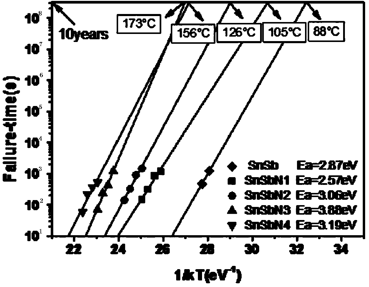
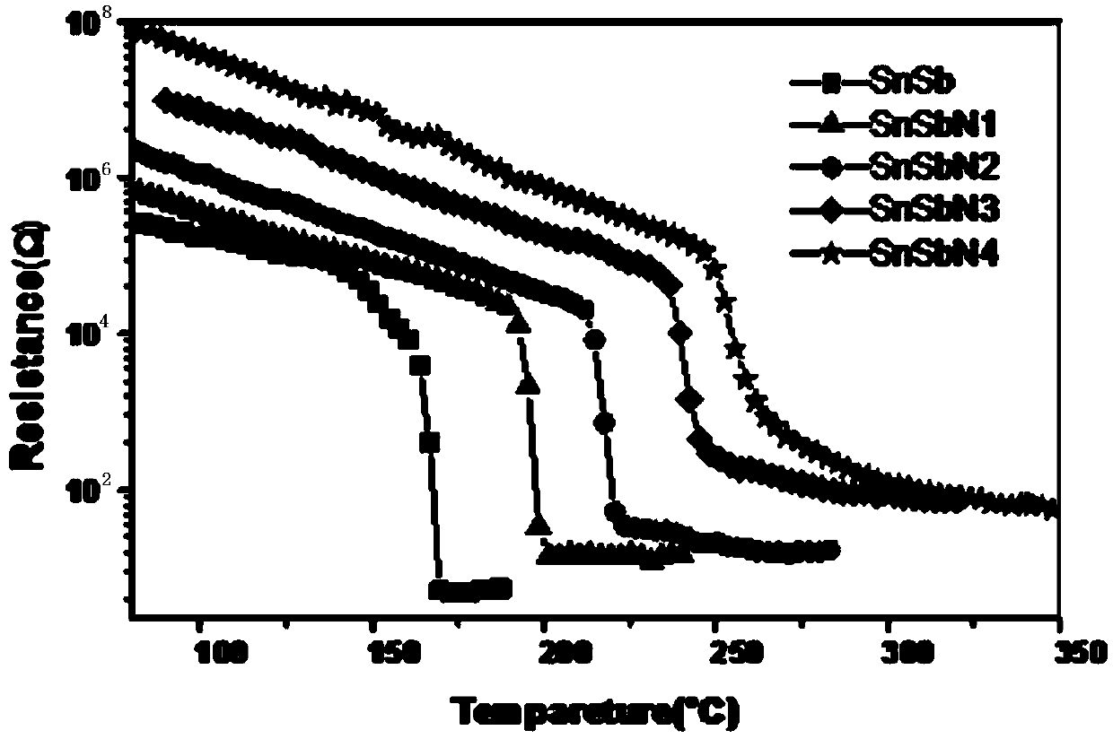
[0024] Nitrogen-doped Sn prepared in this example 15 Sb 85 The structure of the nano phase change thin film material is specifically
[0025] sn 15 Sb 85 N 1 .
[0026] The preparation steps are:
[0027] 1. Clean SiO2 2 / Si(100) substrate, cleaning the surface and back, removing dust particles, organic and inorganic impurities;
[0028] a) strong ultrasonic cleaning in ethanol solution for 10 minutes;
[0029] b) Blow dry the remaining ethanol liquid with a hair dryer on a warm gear for about 30 minutes.
[0030] 2. Preparation of Sn by radio frequency sputtering method 15 Sb 85 N 1 Film preparation:
[0031] a) Install Sn 15 Sb 85 Sputtering target material, the purity of the target material reaches 99.999% (atomic percentage), and the background vacuum is pumped to 5×10 -4 Pa;
[0032] b) Set the sputtering power to 30W;
[0033] c) Using high-purity Ar and high-purity N 2 As the sputtering gas (the volume percent reaches 99.999%), the Ar gas flow rate is ...
Embodiment 2
[0038] Prepare the SnSbNx nano phase change thin film material of the present embodiment, its concrete structure is respectively Sn 15 Sb 85 N 2 , Sn 15 Sb 85 N 3 and Sn 15 Sb 85 N 4 , the preparation method is the same as Example 1, and the nano-Sn 15 Sb 85 N 2 , Sn 15 Sb 85 N 3 and Sn 15 Sb 85 N 4 The sputtering time of the nano phase change thin film material is 100s. Just prepare Sn 15 Sb 85 N 2 The Ar gas flow rate set by the nano phase change thin film material is 28sccm, and the N 2 The flow rate is 2 sccm, and the film preparation methods of other structures can be deduced by analogy.
PUM
| Property | Measurement | Unit |
|---|---|---|
| crystallization temperature | aaaaa | aaaaa |
Abstract
Description
Claims
Application Information
 - R&D
- Intellectual Property
- Life Sciences
- Materials
- Tech Scout
- Unparalleled Data Quality
- Higher Quality Content
- 60% Fewer Hallucinations
Browse by: Latest US Patents, China's latest patents, Technical Efficacy Thesaurus, Application Domain, Technology Topic, Popular Technical Reports.
© 2025 PatSnap. All rights reserved.Legal|Privacy policy|Modern Slavery Act Transparency Statement|Sitemap|About US| Contact US: help@patsnap.com


